Paper Sharing
【Member Papers】1844 V β-Ga₂O₃ Trench-MOS Schottky Barrier Diodes with Improved Electric Field of 5.2 MV/cm
日期:2025-06-20阅读:726
Researchers from the Novel Crystal Technology have published a dissertation titled "1844 V β-Ga2O3 Trench-MOS Schottky Barrier Diodes with Improved Electric Field of 5.2 MV/cm " in ISPSD 2025.
Background
Because of their excellent material properties, especially their dielectric breakdown field, which is several times greater than that for Si, wide-bandgap semiconductors are considered next-generation semiconductors capable of realizing high power, high voltage, high efficiency, high frequency, and high-temperature operation; the range of their applications is now expanding. Among wide-bandgap semiconductors, β-Ga2O3 has been attracting increasing attention over the past decade.
β-Ga2O3, which has an ultrawide-bandgap energy as large as 4.7 eV and a Baliga figure of merit (BFOM), calculated as 3444, is expected to demonstrate high performance exceeding not only that of Si but also those of SiC and GaN. Another noteworthy feature of β-Ga2O3 is that it can be grown in bulk crystal form via edge-defined film-fed growth (EFG), which is a melt-growth method that is potentially cost advantageous. With the development of these methods, 4-inch epitaxial wafers have become commercially available via the halide vapor phase epitaxy (HVPE) method for depositing epitaxial layers; 6-inch epitaxial wafers have also been developed.
Abstract
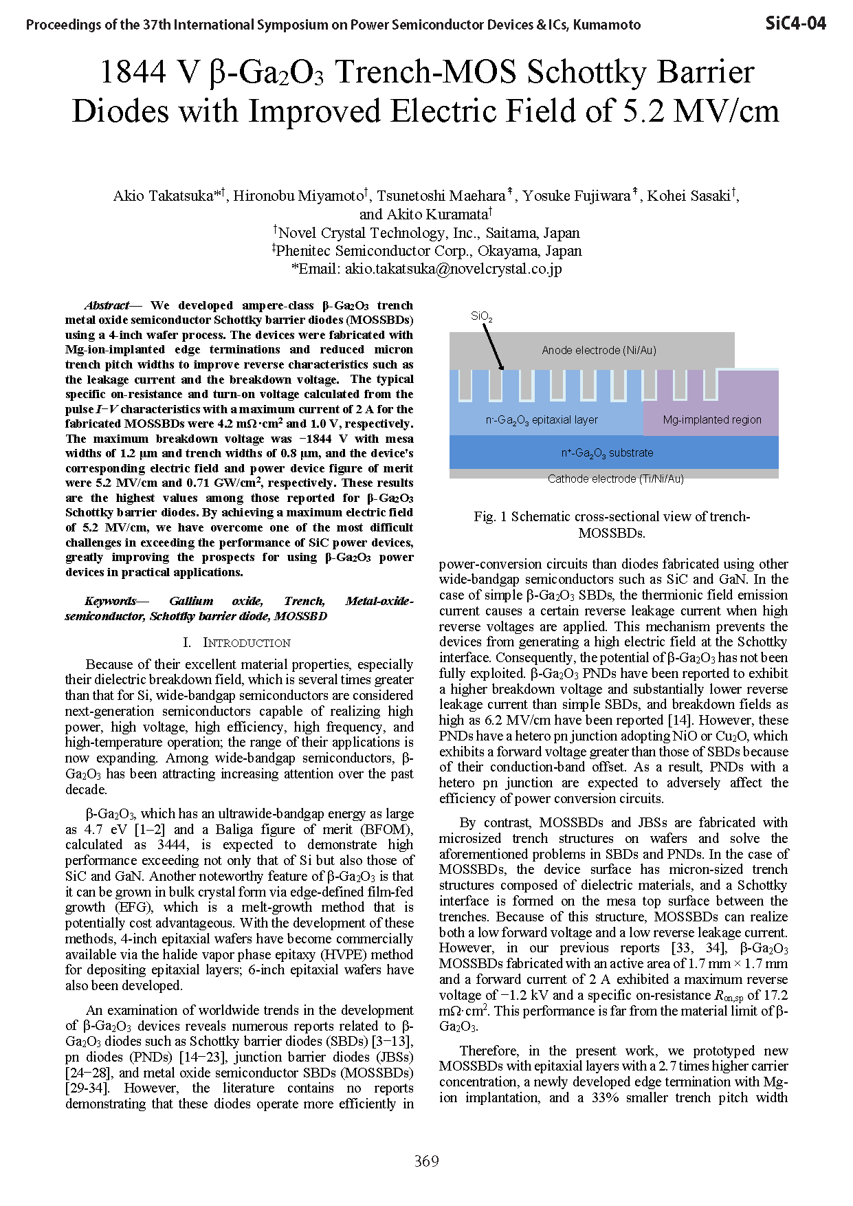
We developed ampere-class β-Ga2O3 trench metal oxide semiconductor Schottky barrier diodes (MOSSBDs) using a 4-inch wafer process. The devices were fabricated with Mg-ion-implanted edge terminations and reduced micron trench pitch widths to improve reverse characteristics such as the leakage current and the breakdown voltage. The typical specific on-resistance and turn-on voltage calculated from the pulse I−V characteristics with a maximum current of 2 A for the fabricated MOSSBDs were 4.2 mΩ·cm2 and 1.0 V, respectively. The maximum breakdown voltage was −1844 V with mesa widths of 1.2 μm and trench widths of 0.8 μm, and the device's corresponding electric field and power device figure of merit were 5.2 MV/cm and 0.71 GW/cm2, respectively. These results are the highest values among those reported for β-Ga2O3 Schottky barrier diodes. By achieving a maximum electric field of 5.2 MV/cm, we have overcome one of the most difficult challenges in exceeding the performance of SiC power devices, greatly improving the prospects for using β-Ga2O3 power devices in practical applications.
Conclusion
We developed ampere-class β-Ga2O3 trench MOSSBDs using a 4-inch wafer process. The devices were fabricated with Mg-ion-implanted edge terminations and reduced micron trench pitch widths to improve reverse characteristics such as their leakage current and VBR. Typical Ron,sp and VON values for the fabricated MOSSBDs, as calculated from the pulse I−V characteristics with a maximum current of 2 A, were 4.2 mΩ·cm2 and 1.0 V, respectively. The maximum obtained VBR was −1844 V with mesa widths of 1.2 μm and trench widths of 0.8 μm, and the corresponding Emax and PFOM were 5.2 MV/cm and 0.71 GW/cm2, respectively. These values are the highest reported for β-Ga2O3-based SBDs. Thus, we confirmed that the ion-implanted edge terminations and the reduced trench pitch widths improve the reverse characteristics of β-Ga2O3 MOSSBDs. By achieving a maximum electric field of 5.2 MV/cm, we have overcome one of the most difficult challenges in exceeding the performance of SiC power devices; the only remaining issues are reducing the parasitic on-resistance of the β-Ga2O3 MOSSBDs. This advance greatly brightens prospects for the practical application of β-Ga2O3 power devices. We are sure that β-Ga2O3 power devices whose performance matches or exceeds that of SiC devices will be realized in the near future.
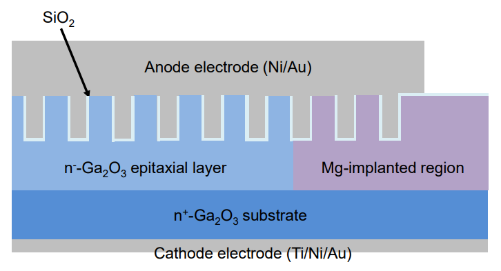
Fig. 1 Schematic cross-sectional view of trench-MOSSBDs.
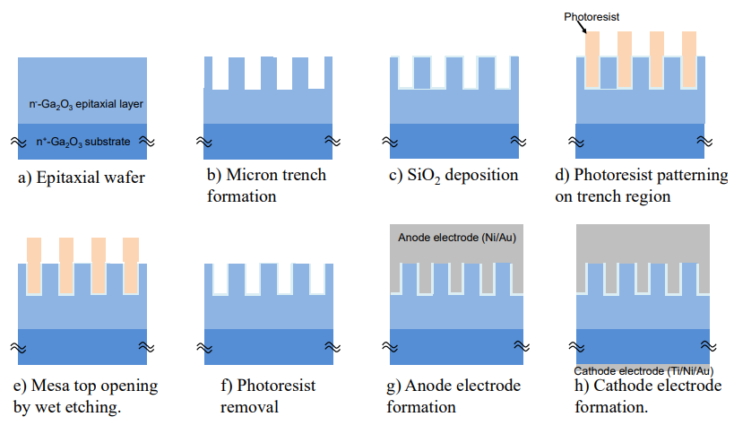
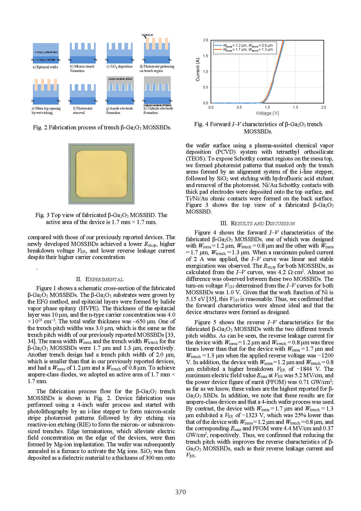
Fig. 2 Fabrication process of trench β-Ga2O3 MOSSBDs.