Paper Sharing
【Domestic Papers】Theoretical Analysis of Vertical β-Ga₂O₃ Schottky Barrier Diodes With p-NiO Field Limiting Rings for High P-FOM Performance
日期:2025-06-20阅读:703
Researchers from the Fuzhou University have published a dissertation titled "Theoretical Analysis of Vertical β-Ga2O3 Schottky Barrier Diodes With p-NiO Field Limiting Rings for High P-FOM Performance" in IEEE Journal of the Electron Devices Society.
Project Support
This work was supported by the Fund of Fujian Provincial Science and Technology Planning Project (No.2022I0006), the Fund of Young and Middle-aged Teacher Education Research Project of Fujian Provincial Department of Education (JAT220026), and the Fund of Science and Technology Major Project of Fujian Province (2022HZ027006).
Introduction
The semiconductor material of Ga2O3 has been widely studied due to its wide bandgap of 4.5-4.9 eV, estimated high critical breakdown electric field (E-field) of 8 MV/cm, and the Baliga’s figure of merit(BFOM=ɛμEC3) is yielded to be around 3000, which outperforms those of other wide bandgap materials such as GaN or SiC. Thus, β-Ga2O3-based power devices have been highly sought after in the high-power community recently. However, due to the self-compensation effect of ntype background carriers in Ga2O3 the lack of shallow level acceptor, and the large effective mass of holes have led to the absence of p-type β-Ga2O3 so far. Therefore, most research attention is paid to unipolar devices, including field effect transistors (FET) and diodes. For diodes, it can be roughly divided into PN junction diode and SBD due to its construction mode. Compared to traditional PN junction diodes, SBD have lower Von and faster reverse recovery times, so them being commonly used as high-speed switching devices.
Abstract
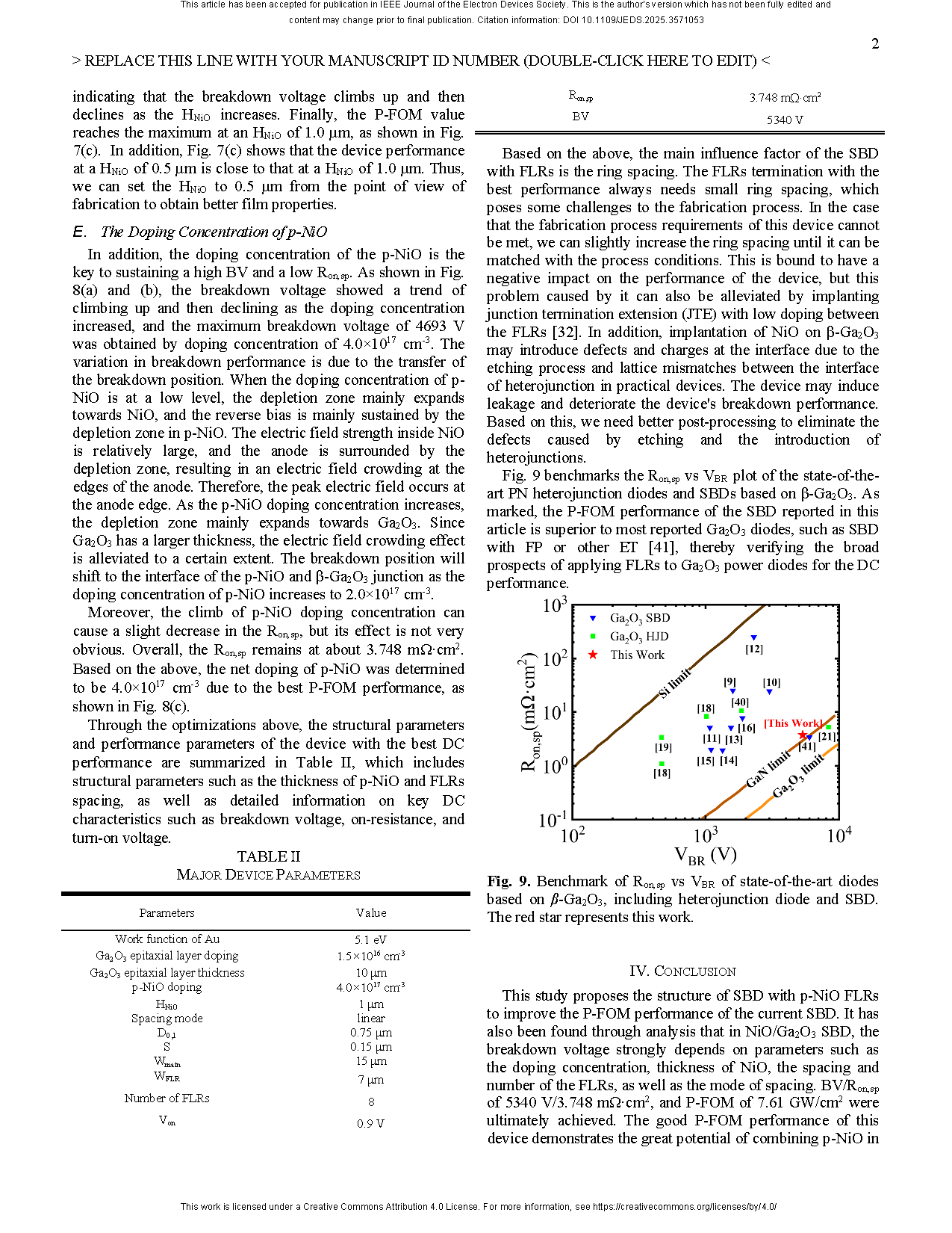
Power devices based on Ga2O3 have been widely studied in recent years. Due to the absence of the p-Ga2O3, the performance of the power devices based on Ga2O3 was largely limited. To get better performance, many Ga2O3 Schottky Barrier Diodes (SBD) with edge termination (ET) were proposed. In this work, p-NiO field limiting rings (FLRs) are implanted into Ga2O3 SBD to improve the power figure of merit (P-FOM) and reduce the complexity of the current high-performance edge termination structure manufacturing process. The implantation of the FLRs can weaken the peak electric field strength and extend the depletion zone in the horizontal direction. Further exploring the influence of some parameters of the device on device performance through TCAD simulation, the breakdown voltage (BV)/specific on-resistance (Ron,sp) of SBD with FLRs is up to 5340 V/3.748 mΩ·cm2, and P-FOM = BV2/Ron,sp can reach 7.61 GW/cm2, and turn-on voltage (Von) of 0.9 V is achieved. The manufacturing process of the presented Ga2O3 SBD with p-NiO FLRs is relatively simple compared to devices with approximate P-FOM values. This kind of Ga2O3 SBD with FLRs has great promise for future high-power applications.
Conclusion
This study proposes the structure of SBD with p-NiO FLRs to improve the P-FOM performance of the current SBD. It has also been found through analysis that in NiO/Ga2O3 SBD, the breakdown voltage strongly depends on parameters such as the doping concentration, thickness of NiO, the spacing and number of the FLRs, as well as the mode of spacing. BV/Ron,sp of 5340 V/3.748 mΩ·cm2, and P-FOM of 7.61 GW/cm2 were ultimately achieved. The good P-FOM performance of this device demonstrates the great potential of combining p-NiO in Ga2O3 power electronic devices.
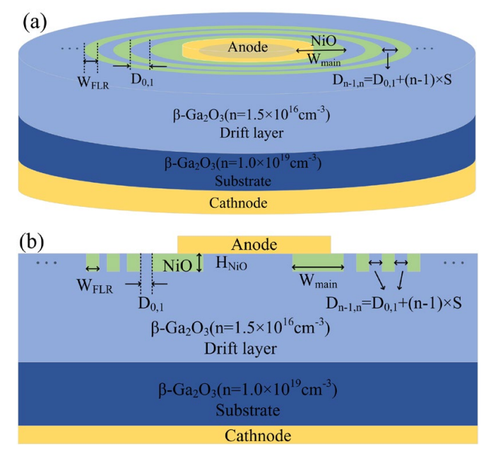
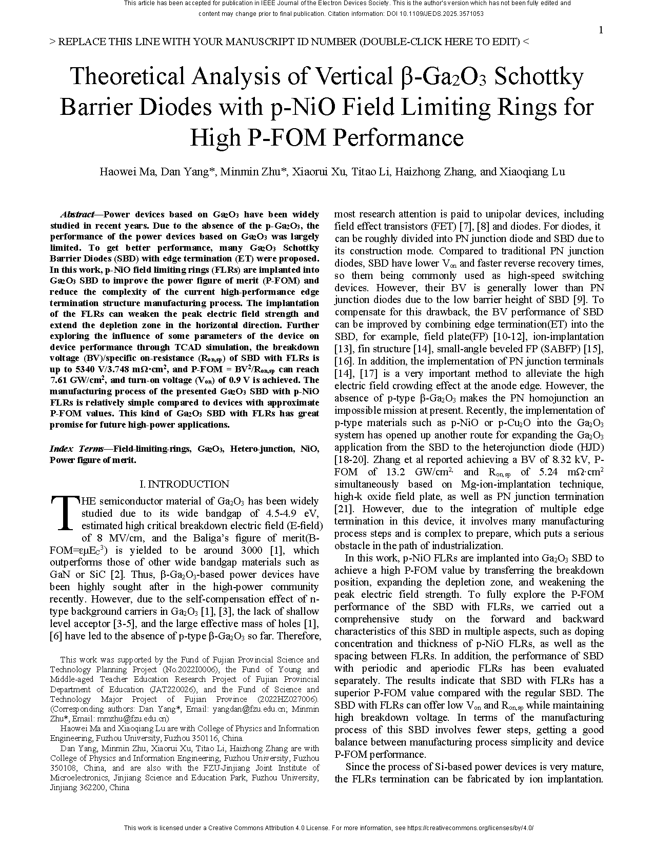
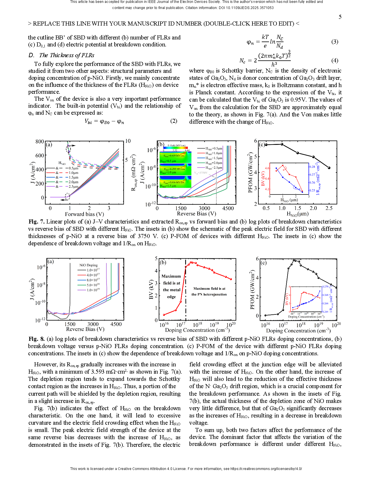
Fig. 1. (a) 3D and (b) 2D cross-sectional schematic of the SBD with FLR.
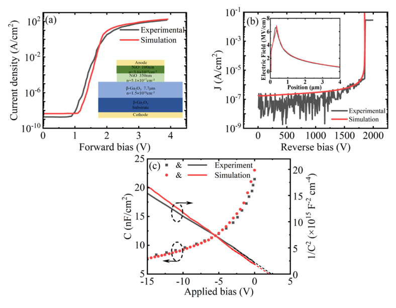
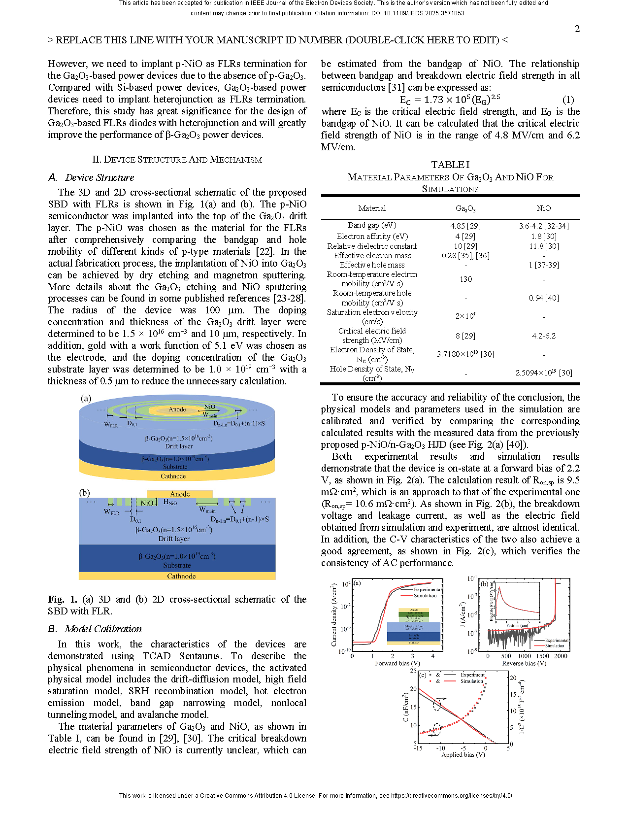
图2. 垂直 NiO/β-Ga2O3 HJD 的(a)正向 J-V 特性和(b)反向 J-V 特性的截面示意图。图(a)中的插图显示了垂直 NiO/β-Ga2O3 HJD 在反向偏压为 0.94 kV 时的二维电场分布。(c) 该 HJD 在 100 kHz 频率下测得的 C-V 特性曲线及 1/C2-V 特性曲线。
DOI:
doi.org/10.1109/JEDS.2025.3571053