Paper Sharing
【Member Papers】Xi’an Jiaotong University --- The γ-Ray TID Effect and Irradiation Damage Recovery on β-Ga₂O₃/Al₂O₃ MOSCAPs
日期:2025-06-20阅读:725
Researchers from the Xi’an Jiaotong University have published a dissertation titled "The γ-Ray TID Effect and Irradiation Damage Recovery on β-Ga2O3/Al2O3 MOSCAPs" in IEEE Transactions on Electron Devices.
Project support
This work was supported in part by the Joint Funds of the National Natural Science Foundation of China under Grant U23A20367 and in part by the National Natural Science Foundation of China under Grant 62204198.
Background
Beat-gallium oxide (β-Ga2O3) material has garnered considerable research interest in the fields of power electronics and optoelectronic devices, for the remarkable properties, such as a high breakdown electric field strength of up to 8 MV cm−1 and a large bandgap of 4.8–4.9 eV, which allows devices to operate reliably under challenging conditions, such as high voltage and high temperature. Additionally, due to the high displacement energies of Ga and O atoms β-Ga2O3-baseddevices are also suitable for applications in complex radiation environments, including outer space and nuclear industry. Currently, the radiation effects of high-energy protons, electrons, γ -rays, and neutrons on β-Ga2O3-based metal–oxide–semiconductor (MOS) devices and diode devices have been studied. Based on current reports, the oxide layer materials and interfaces significantly affect the electrical characteristics of β-Ga2O3-based MOS structures, and they are also more susceptible to radiation damage. However, previous studies on total ionizing dose (TID) effects have predominantly focused on defect behaviors in β-Ga2O3 semiconductor materials, with relatively less analysis on the impact of the oxide layer and the interface between the oxide layer and the β-Ga2O3 material. Therefore, further research is needed to analyze the effects of irradiation damage on β-Ga2O3-based MOS devices.
Abstract
In this study, the impact of γ -ray total ionizing dose (TID) irradiation on the electrical performance of beta-gallium oxide (β-Ga2O3)/Al2O3 MOSCAPs was investigated, and a new irradiation damage recovery method was also proposed using the supercritical N2O (SCN2O) fluid postoxidation annealing (POA) process. After a cumulative γ -ray dose of 1.108 Mrad (SiO2), the net carrier concentration (Nd) decreased by 28.7%, and the interface state density (Dit) increased from 4.41×10¹¹ to 5.12×10¹¹ eV−1 cm−2, according to the frequency-dependent capacitance-voltage (C–V) measurements. Meanwhile, the effective trapped charge density (Neff) was reduced from −1.82×10¹² to −1.37×10¹² eV−1 cm−2, leading to a decreased flat-band voltage (Vfb), which was attributed to the formation of positively charged oxide trapped charge (Not). What is more, the forward leakage current density increased by ten times, and a 9.5% decrease in the breakdown voltage (Vbr) was observed according to the current-voltage (I–V) measurements. Moreover, the leakage current analysis indicated that the changes in the I–V characteristics were primarily caused by variations in Dit and Not. In addition, after the SCN2O POA process at 120 °C, the damages of the irradiated device can be repaired. Specifically, the material properties, such as Nd, Dit, and Neff, and the electrical properties of Vbr and the forward leakage current density recovered to the preirradiation level. The results demonstrated that the low-temperature SCN2O POA process is promising for repairing TID irradiation damage in β-Ga2O3/Al2O3⋅ devices.
Conclusion
In this study, the impact of 1.108-Mrad (SiO2) γ -ray irradiation on the electrical performance of β-Ga2O3/Al2O3 MOSCAPs was investigated, and a novel low-temperature SCN2O POA was proposed to repair irradiation-induced damage. After irradiation, Nd decreased by 28.7%, and Dit increased from 4.41 × 10¹¹ to 5.12 × 10¹¹ eV−1 cm−2. Neff decreased from −1.82 × 10¹² to −1.37 × 10¹² eV−1 cm−2, attributed to the formation of Not and led to a decreased Vfb. What is more, the leakage current density increased by ten times and a 9.5% decrease in Vbr. The leakage current analysis indicated that irradiation-induced traps and charges were the primary causes of the reduction in Vbr and the increase in the leakage current of the MOSCAPs. Besides, after SCN2O POA, the material properties and the electric properties trended to recover to the preirradiation states, demonstrating that SCN2O POA was useful for repairing the TID radiation effects in the β-Ga2O3/Al2O3 MOSCAPs. Specifically, Nd, Dit, and Neff of the irradiated material recovered to 2.36 × 1016 cm−3, 4.40 × 10¹¹ eV−1 cm−2, and −2.15 × 10¹² eV−1 cm−2, respectively, as the preirradiation state. Moreover, the leakage current, influenced by radiation-induced defects and traps, was governed by the PF mechanism at lower electric fields and by the TAT mechanism at higher fields. In short, these findings provide valuable insights into the repair of irradiation-induced damage and the enhancement of β-Ga2O3-based MOS devices for radiation environments. In the future, the SCF will be introduced into the Ga2O3-based device design and preparation in a more targeted way to enhance the radiation resistance.
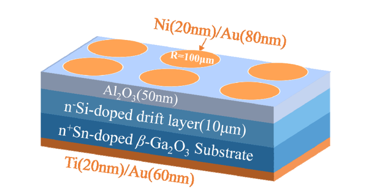
Fig. 1. Schematic view of β-Ga2O3/Al2O3 MOSCAPs.
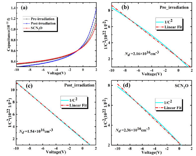
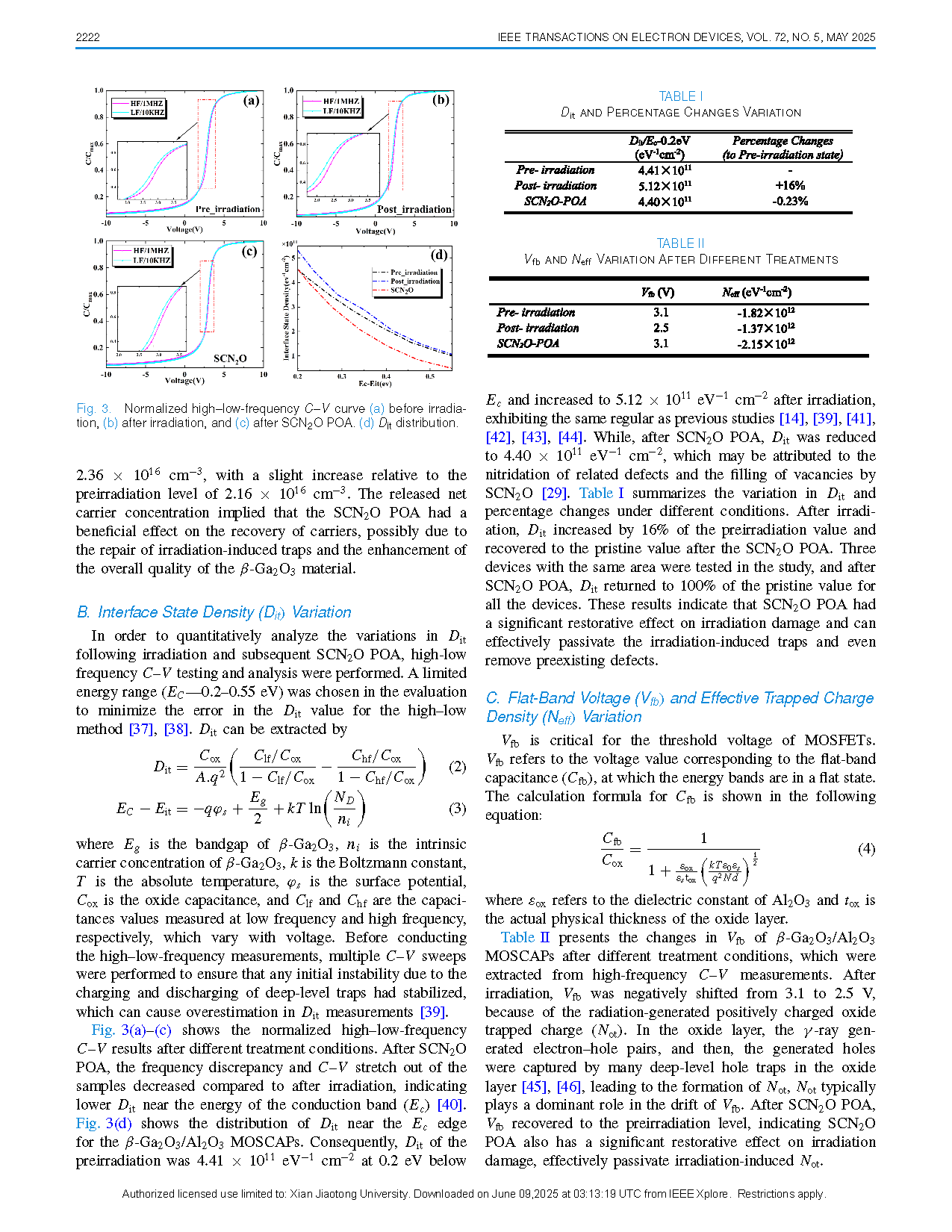
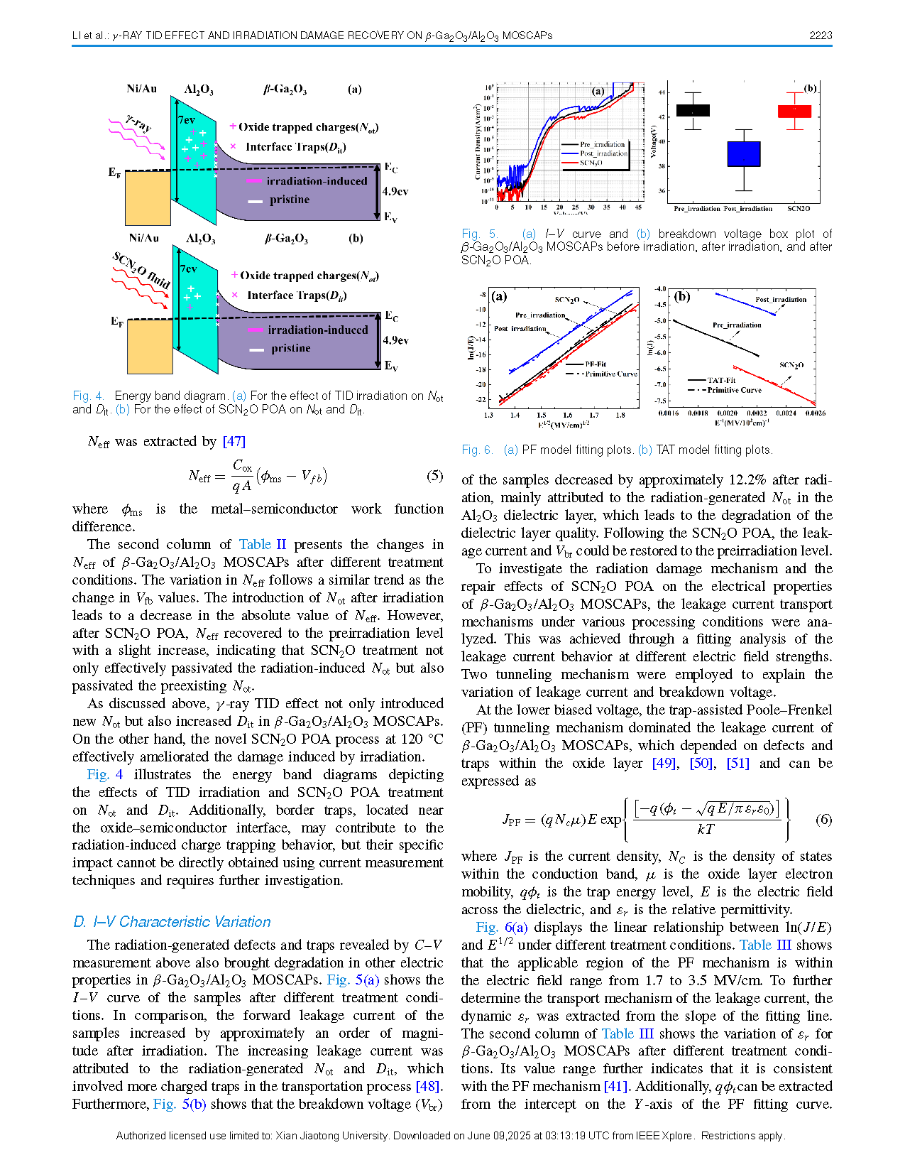
Fig. 2. (a) C–V curves at different conditions. 1/C2–V curve (b) before irradiation and (c) after irradiation. (d) SCN2O POA treatment.
DOI:
doi.org/10.1109/JSEN.2025.3560314