Paper Sharing
【Domestic Papers】Integrating photodetection and neuromorphic vision in ALD-grown amorphous Ga₂O₃ thin films via bias-voltage modulation
日期:2025-07-03阅读:656
Researchers from the Nanjing University of Science and Technology have published a dissertation titled "Integrating photodetection and neuromorphic vision in ALD-grown amorphous Ga2O3 thin films via bias-voltage modulation" in Optics Express.
Project Support
Fundamental Research Funds for the Central Universities (30923011002).
Background
Gallium oxide (Ga2O3), an ultra-wide-bandgap semiconductor (UWBG) material, has attracted significant research interest due to its exceptional properties, including an ultra-wide bandgap, high refractive index, and superior mechanical hardness. These characteristics make it highly suitable for diverse applications such as sensing systems, memory devices, power electronics, and photodetectors. Recently, Ga2O3 based optoelectronic artificial synapses have attracted widespread attentions, which can be utilized in the fields of image recognition and information encryption. In particular, Ga2O3 is an excellent candidate for deep ultraviolet (DUV) photodetection, owing to its tunable bandgap (4.5-5.3 eV) . This wide bandgap ensures high transparency in the visible spectrum while enabling strong absorption of deep ultraviolet radiation.
Abstract
We demonstrate what we believe to be a new atomic layer deposition (ALD) process utilizing gallium chloride (GaCl3) and water vapor as complementary precursors for synthesizing high-quality Ga2O3 thin films. The developed process enables the growth of ultrasmooth amorphous Ga2O3 layers with sub-nanometer surface roughness and an ultrawide bandgap of 5.29 eV, ideal for deep-ultraviolet (DUV) photonic applications. Metal-semiconductor-metal (MSM) photodetectors employing the Au/ Ga2O3/Au architecture achieve exceptional performance metrics, including an outstanding photocurrent ratio of 98.36 under 254 nm illumination and ultrafast response characteristics (0.23 s rise/0.25 s decay times). The devices exhibit unique bias-tunable dual-mode operation: low-voltage operation enables conventional fast-response photodetection, while high bias conditions induce persistent photoconductivity effects. This voltage-dependent reconfigurability allows effective emulation of neurobiological functions, particularly demonstrating paired-pulse facilitation and replicating sophisticated learning-forgetting-relearning cognitive processes. Our findings establish ALD-grown Ga2O3 as a versatile platform for developing multifunctional optoelectronic systems that synergistically integrate high-performance DUV detection with neuromorphic computing capabilities, paving the way for next-generation reconfigurable optical memory devices and bio-inspired visual processing architectures.
Conclusion
In this work, we demonstrate the growth of high-quality Ga2O3 thin films via thermal ALD using GaCl3 and H2O as a new precursor combination. The self-limiting, layer-by-layer growth characteristics of ALD enable precise thickness control and yield films with excellent uniformity and low surface roughness. Optical characterization reveals strong deep-ultraviolet absorption with a tunable bandgap ranging from 4.5 to 5.5 eV. Fabricated MSM photodetectors exhibit outstanding performance metrics under 1 V bias, including a high PDCR of 98.36 and fast response characteristics (rise time τr1 = 0.23 s; decay time τd1 = 0.25 s). Notably, the device demonstrates bias-voltage-tunable multifunctionality, enabling reversible switching between conventional photodetection and neuromorphic visual sensing modes. At high bias voltage, biological synaptic behaviors such as paired-pulse facilitation and learning-forgetting-relearning processes can be realized. These results highlight the significant potential of ALD-derived Ga2O3 thin films for developing next-generation reconfigurable optoelectronic devices with integrated functionalities.
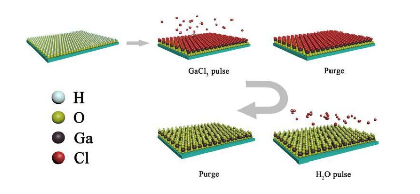
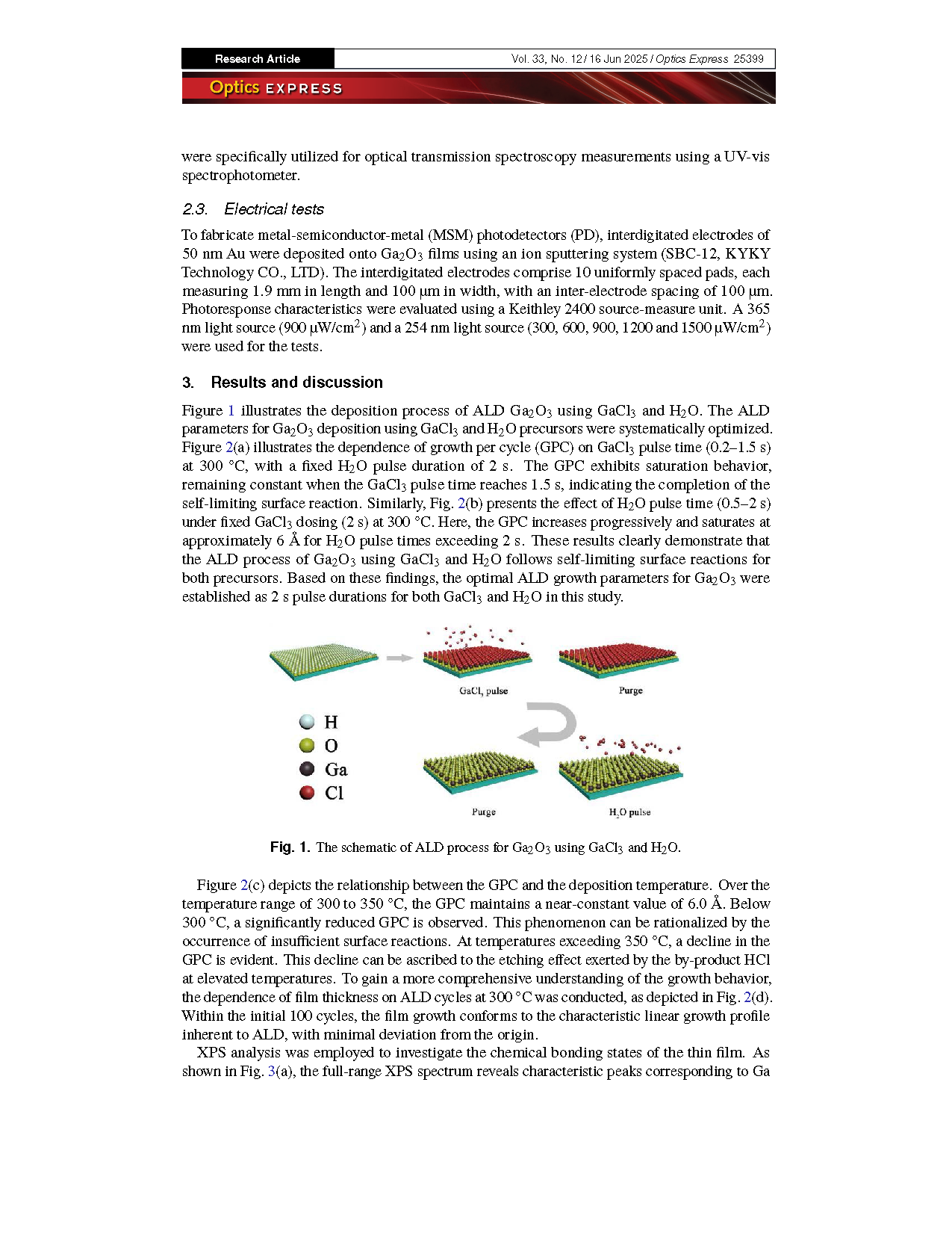
Fig. 1. The schematic of ALD process for Ga2O3 using GaCl3 and H2O.
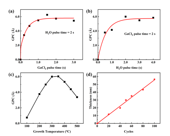
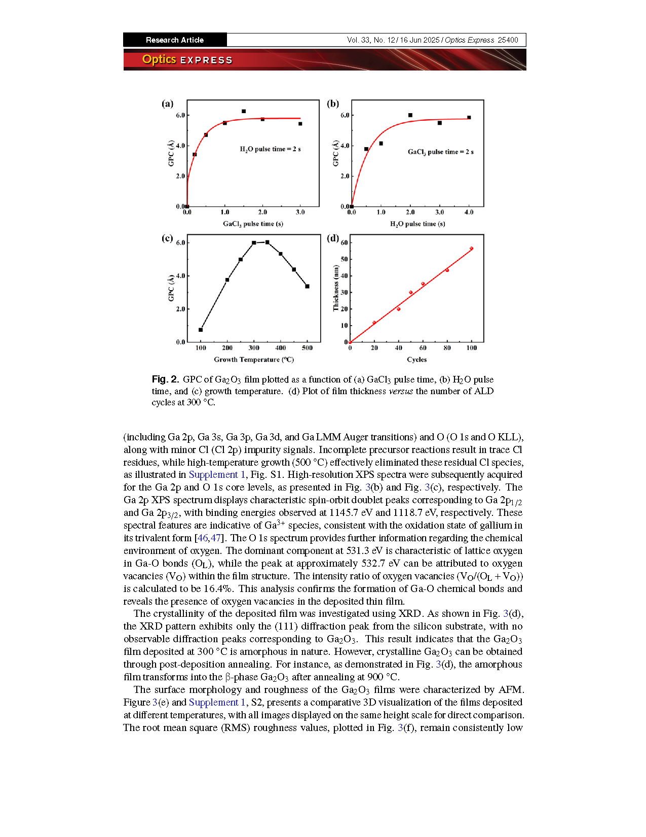
Fig. 2. GPC of Ga2O3 film plotted as a function of (a) GaCl3 pulse time, (b) H2O pulse time, and (c) growth temperature. (d) Plot of film thickness versus the number of ALD cycles at 300 °C.
DOI:
doi.org/10.1364/OE.564628