


News Trends
【World Express】FLOSFIA Achieves the World's First Breakthrough, Successfully Overcoming the Technical Difficulties of Gallium Oxide P-Type Layer
日期:2025-07-03阅读:1126
Recently, according to FLOSFIA, normally off (Normally-off) high-current (over 10 A) operation based on Gallium Oxide (α-Ga2O3) MOSFETs has been successfully achieved. The new achievement was made through the successful improvement of the P-layer (conductive P-type semiconductor layer), which has long been regarded as the biggest technical difficulty in the development of Gallium Oxide power semiconductors.
Overcoming the "Biggest Barrier" for Practical Mass Production
In the process of manufacturing Gallium Oxide semiconductor MOSFET structures, the p layer plays an essential and crucial role in bringing out the high-performance potential of the material. According to FLOSFIA, most other research institutions, due to the high technical difficulty at present, have not adopted the p layer but have avoided the problem by simplifying the device structure.
FLOSFIA believes that in order to fully leverage the high performance of Gallium Oxide materials (high withstand voltage/low loss) and achieve practical mass production equipment manufacturing, it is highly necessary to adopt a P-layer device structure. Therefore, the company's unique Mier-Dry technology has promoted the formation technology of the p layer in Gallium Oxide. Based on this, FLOSFIA has achieved product-level sample validation in JBS (Junction Barrier Schottky) structured diodes.
This time, FLOSFIA took on the more technically challenging application of the p-layer MOSFET structure by highly improving its own technology, developed a new MOS structure formation process, and successfully integrated it into the device. FLOSFIA stated that this is the world's first major breakthrough in achieving both the normally-off type and high current characteristics in Gallium Oxide MOSFETs.
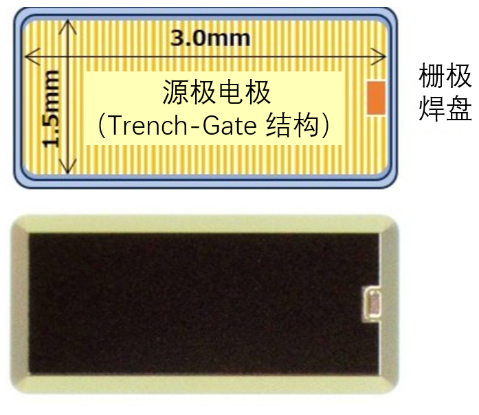
Figure 1. Prototype circuit diagram of MOSFET (top) and chip photo (bottom), source: FLOSFIA
14.3A Drain Current is Achieved at A 15 V Gate Voltage
FLOSFIA has successfully produced high-quality α-Ga2O3 epitaxial layers using its independently developed Mier-Dry technology, which are used to manufacture devices with a 600V withstand voltage rating. Using Trench-Gate MOSFETs that are conducive to miniaturization and low on-resistance, p layers were applied to reduce the channel region resistance, which accounts for a large proportion of the MOSFET's on-resistance, and a new type of MOS structure process was developed. In addition, by transferring an ultra-thin α-Ga2O3 MOSFET with a thickness of approximately 10 μm onto a metal support substrate, a vertical device structure with high electrical conductivity and heat dissipation characteristics comparable to those of Silicon Carbide (SiC) has been achieved.
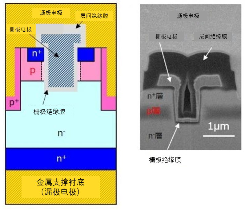
Figure 2. Cross-sectional diagram of the Trench-Gate MOSFET under development (left) and electron microscope image of the fabricated Trench-Gate section (right), source: FLOSFIA
The final fabricated α-Ga2O3 MOSFET achieved an on-state characteristic with a leakage current of 14.3A at a gate voltage of 15 V and no drain current at a gate voltage of 0 V, achieving an ideal normally-off type characteristic. The characteristic on-resistance in the on-region of the device is 17mΩ · cm2. FLOSFIA stated that in the future, it will pursue low-loss performance surpassing that of SiC-MOSFETs by further improving the MOS structure process and miniaturizing the trench gate structure.
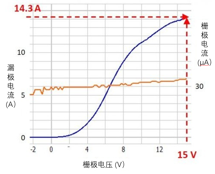
Figure 3 Drain current-gate voltage characteristics, source: FLOSFIA
Moving Towards Mass Production, with the Goal of Full Launch in 2026
FLOSFIA stated that it will take this achievement as a foundation to further accelerate the research and development work on the introduction of withstand voltage structures, high withstand voltage, and the reliability guarantee required for productization. The company is currently building a million-per-month production technology platform capable of producing millions per month , centered around its home plant near Kyoto University, and plans to start full-scale production after fiscal year 2026.
