Paper Sharing
【Member Papers】First Demonstration of CuCrO₂/β-Ga₂O₃ p-n Heterojunction Diode With High Breakdown Voltage and Low Leakage Current
日期:2025-07-03阅读:656
Researchers from the Xiamen University have published a dissertation titled "First Demonstration of CuCrO2/β-Ga2O3 p-n Heterojunction Diode With High Breakdown Voltage and Low Leakage Current" in IEEE Transactions on Electron Devices.
Project Support
This work was supported in part by the National Natural Science Foundation of China under Grant 62171396 and in part by Shenzhen Science and Technology Program under Grant JCYJ20240813145617023.
Background
Ultrawide bandgap (UWB) semiconductors are capable of sustaining higher critical fields, allowing for higher blocking voltages at lower resistances, and therefore, they hold great promise of better conversion efficiency and maintaining higher voltages for modern industrial and electronics products. β-gallium oxide (β-Ga2O3) has a bandgap of 4.8 eV, a high critical field of 8 MV/cm, and a high Baliga’s figure of merit (3400), making β-Ga2O3 power devices enjoy predominant strength in UWB semiconductor devices. The past five years have seen great efforts made to improve device performance and push the limits in such power devices as Schottky barrier diodes (SBDs) and metal–oxide–semiconductor field-effect transistors (MOSFETs). Theoretically, β-Ga2O3 SBDs can achieve an ultrahigh breakdown voltage (Vbr) up to 8.32 kV while maintaining a low specific ON-resistance (Ron,sp) of 5.24 mΩ· cm2. However, the current performance of the device, especially the representative device parameter power figure of merit (PFOM), remains significantly below the expected material limits.
Abstract
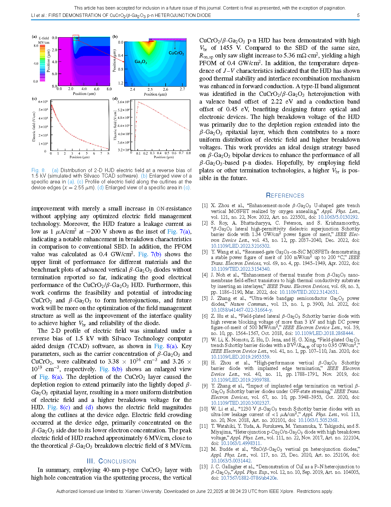
We demonstrate for the first time a high-performance CuCrO2/β-gallium oxide (β-Ga2O3) p-n heterojunction diode (HJD) with high breakdown voltage and low leakage current. Without any composite termination structure, the CuCrO2/β-Ga2O3 HJD reached a high breakdown voltage of 1.46 kV with low leakage current of 10 μA/cm2, which is almost four times improvement over the traditional β-Ga2O3 Schottky barrier diodes (SBDs). Simultaneously, the HJD exhibited a turn-on voltage of 1.62 V and a relatively low specific on-resistance of 5.36 mΩ⋅cm2, yielding a power figure of merit (PFOM) of 0.4 GW/cm2. The measurements of temperature-dependent current density–voltage (J–V) showed that the HJD exhibited good thermal reliability and carrier transport got increasingly dominated by interface recombination at higher temperatures. Furthermore, a type-II band alignment was identified in the CuCrO2/ β-Ga2O3 heterojunction with a valence band offset of 2.22 eV and a conduction band offset of 0.45 eV, respectively, as determined by the X-ray photoelectron spectroscopy (XPS) characterizations. Technology computer aided design (TCAD) simulations indicated that the depletion region primarily extended into the Ga2O3 epitaxial region due to the full depletion of the p-CuCrO2 layer, which contributes to a more uniform distribution of electric field and higher breakdown voltages. Evidently, these results indicate that the formation of heterojunction by introducing a p-CuCrO2 layer is feasible and effective for achieving high-performance and improving manufacturing of β-Ga2O3 bipolar power diodes.
Conclusion
In summary, employing 40-nm p-type CuCrO2 layer with high hole concentration via the sputtering process, the vertical CuCrO2/β-Ga2O3 p-n HJD has been demonstrated with high Vbr of 1455 V. Compared to the SBD of the same size, Ron,sp only saw slight increase to 5.36 m·cm2 , yielding a high PFOM of 0.4 GW/cm2 . In addition, the temperature dependence of J–V characteristics indicated that the HJD has shown good thermal stability and interface recombination mechanism was enhanced in forward conduction. A type-II band alignment was identified in the CuCrO2/β-Ga2O3 heterojunction with a valence band offset of 2.22 eV and a conduction band offset of 0.45 eV, benefiting designing future optical and electronic devices. The high breakdown voltage of the HJD was primarily due to the depletion region extended into the β-Ga2O3 epitaxial layer, which then contributes to a more uniform distribution of electric field and higher breakdown voltages. This work provides an ideal design strategy based on β-Ga2O3 bipolar devices to enhance the performance of all β-Ga2O3-based p-n diodes. Hopefully, by employing field plates or other termination technologies, a higher Vbr is possible in the future.
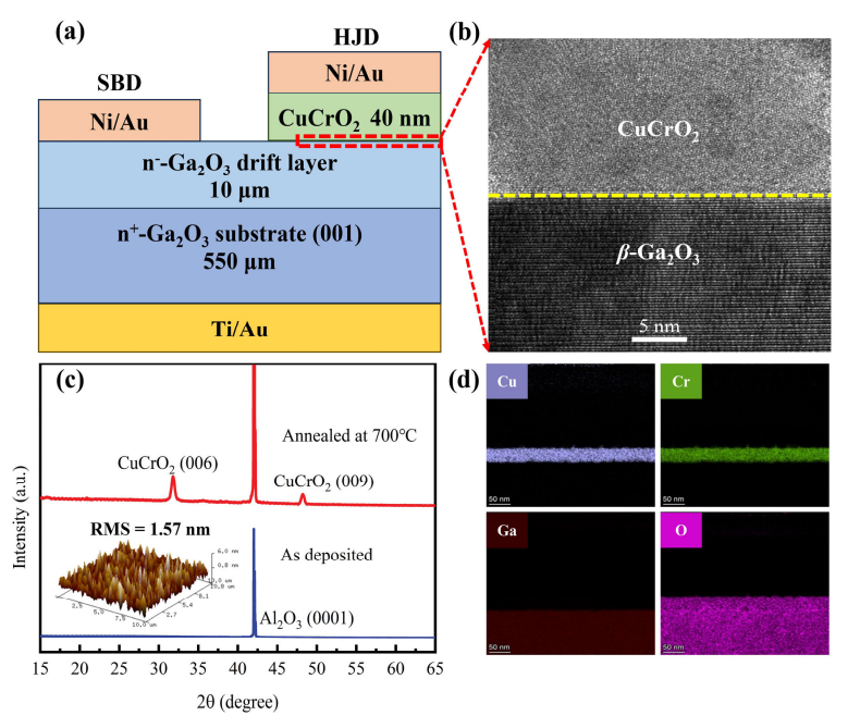
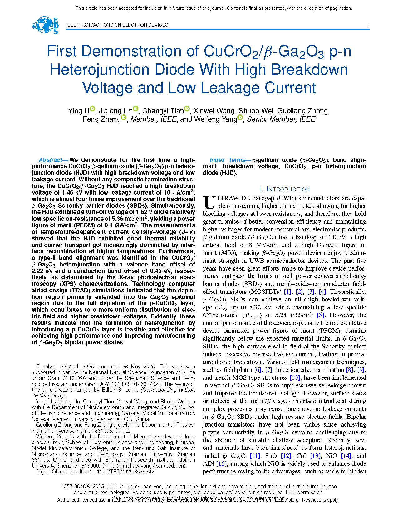
Fig. 1. (a) Cross section schematic of the (left) conventional SBD and (right) the CuCrO2/β-Ga2O3 p-n HJD and (b) corresponding HRTEM image of the CuCrO2/β-Ga2O3 interface. (c) X-ray diffraction (XRD) patterns and AFM scan (inset) of the sputtered CuCrO2 film. (d) Elements characterized with EDS mapping image of the CuCrO2/β-Ga2O3 interface.
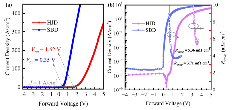
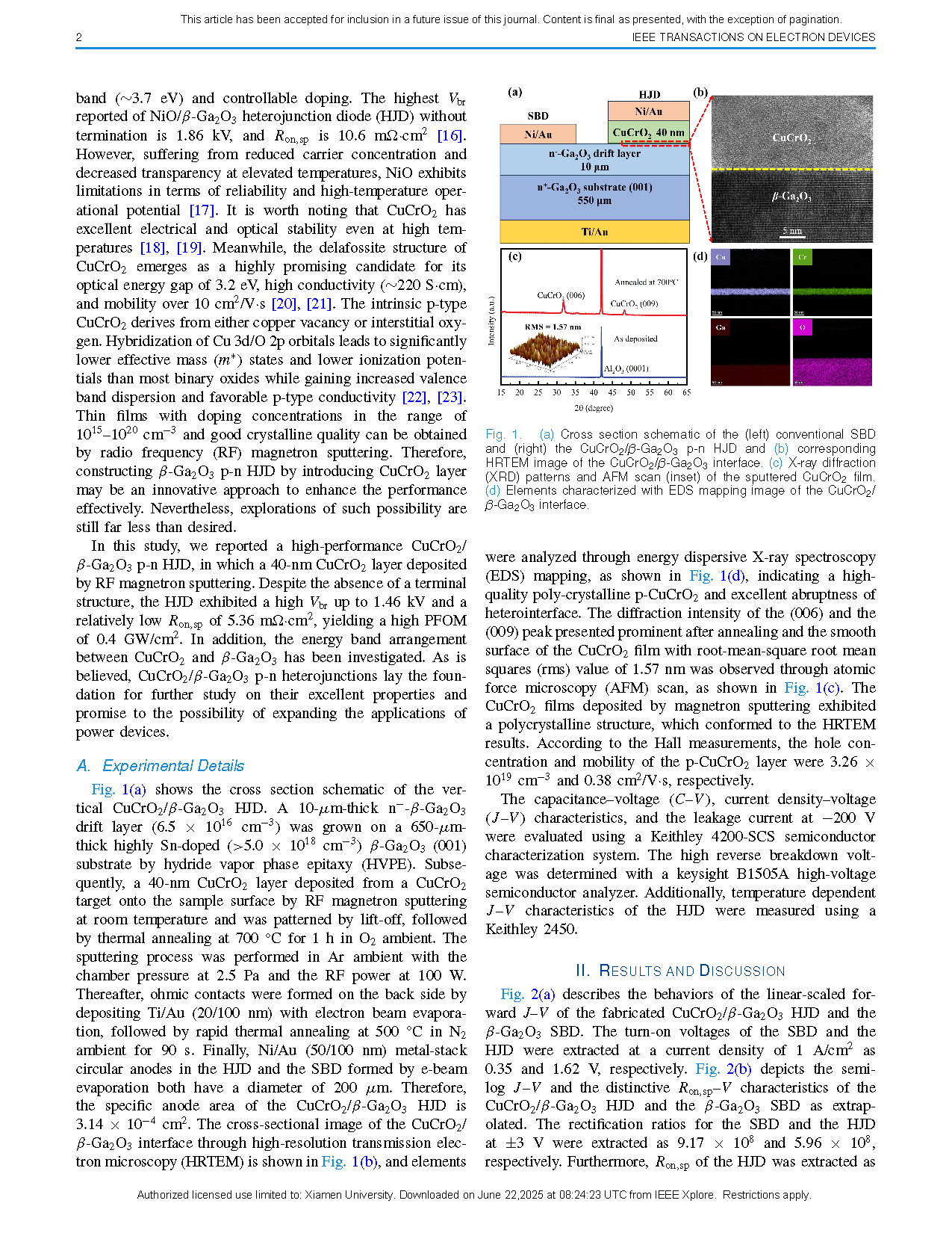
Fig. 2. (a) Linear plots of the J–V and (b) semi-logarithmic plots of the J–V characteristics and the extracted Ron,sp versus the forward bias for the fabricated CuCrO2/β-Ga2O3 p-n HJD and the β-Ga2O3 SBD.
DOI:
doi.org/10.1109/TED.2025.3575742