Paper Sharing
【Member Papers】Precise thermal dissipation of Ga₂O₃ devices integrated with diamond heat spreading layer
日期:2025-07-03阅读:647
Researchers from the Xi’an University of Technology and Xidian University have published a dissertation titled "Precise thermal dissipation of Ga2O3 devices integrated with diamond heat spreading layer" in Materials Today Communications.
Project Support
This work was supported by the National Natural Science Foundation of China (Grant Nos. 62404180, 62474139, 62171367, 92364101), Science and technology planning project of Xi’an (No. 2023JH-GXRC0122) and Young Talent Fund of Xi’an Association for Science and Technology (No. 0959202513045).
Background
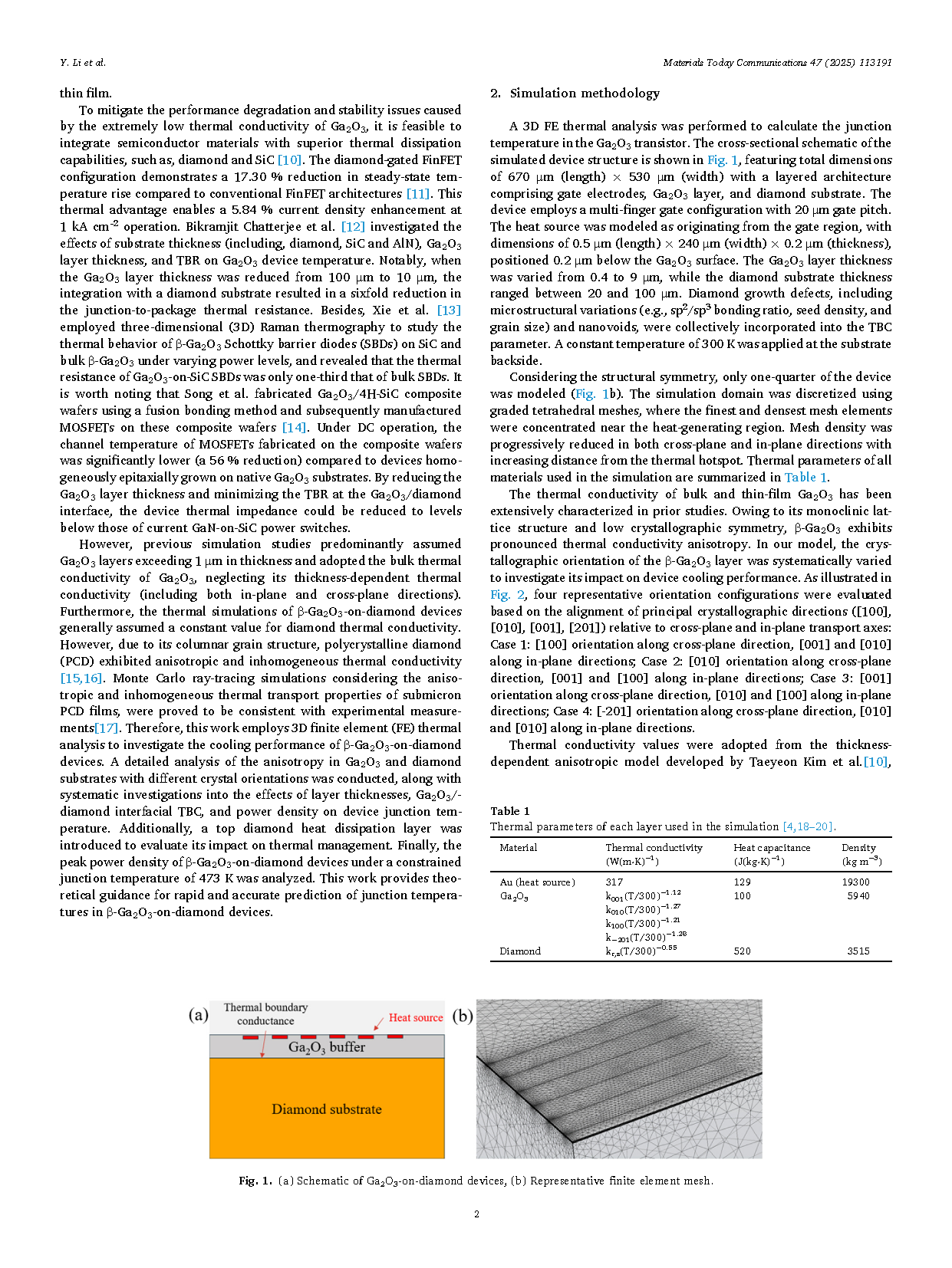
β-phase gallium oxide (β-Ga2O3) has increasingly emerged as a focal point in the emerging power electronics technology, attributed to its superior electrical characteristics, such as an exceptionally wide bandgap (∼4.8 eV) and high critical breakdown electric field (∼8 MV cm⁻1). The Baliga figure of merit (BFOM) of β-Ga2O3, is approximately 10 times and 4 times higher than that of 4H-SiC and GaN, respectively. The enhanced figures of merit, combined with the relatively low production costs, and the commercial availability of large-size β-Ga2O3 single-crystal substrates, impel β-Ga2O3 as a highly promising candidate material for high-voltage switching and radio-frequency electronic devices.
Abstract
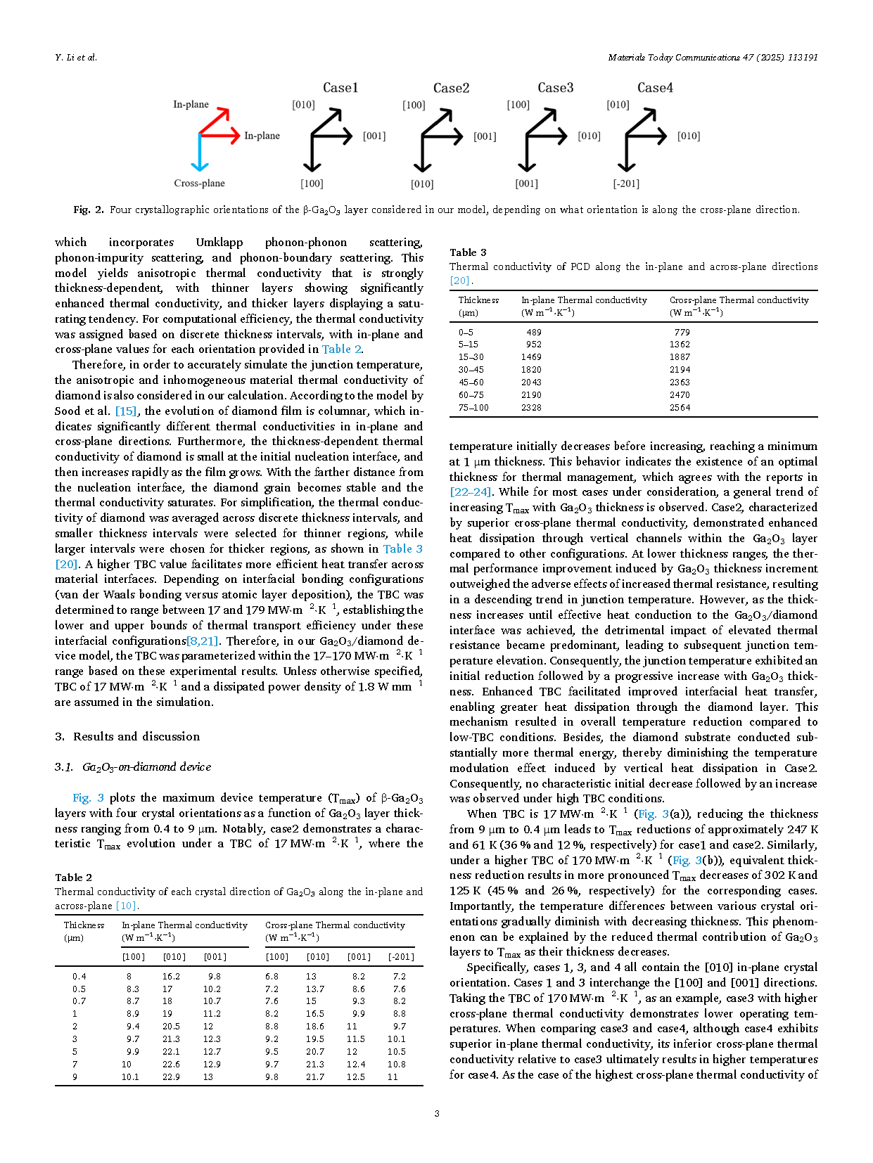
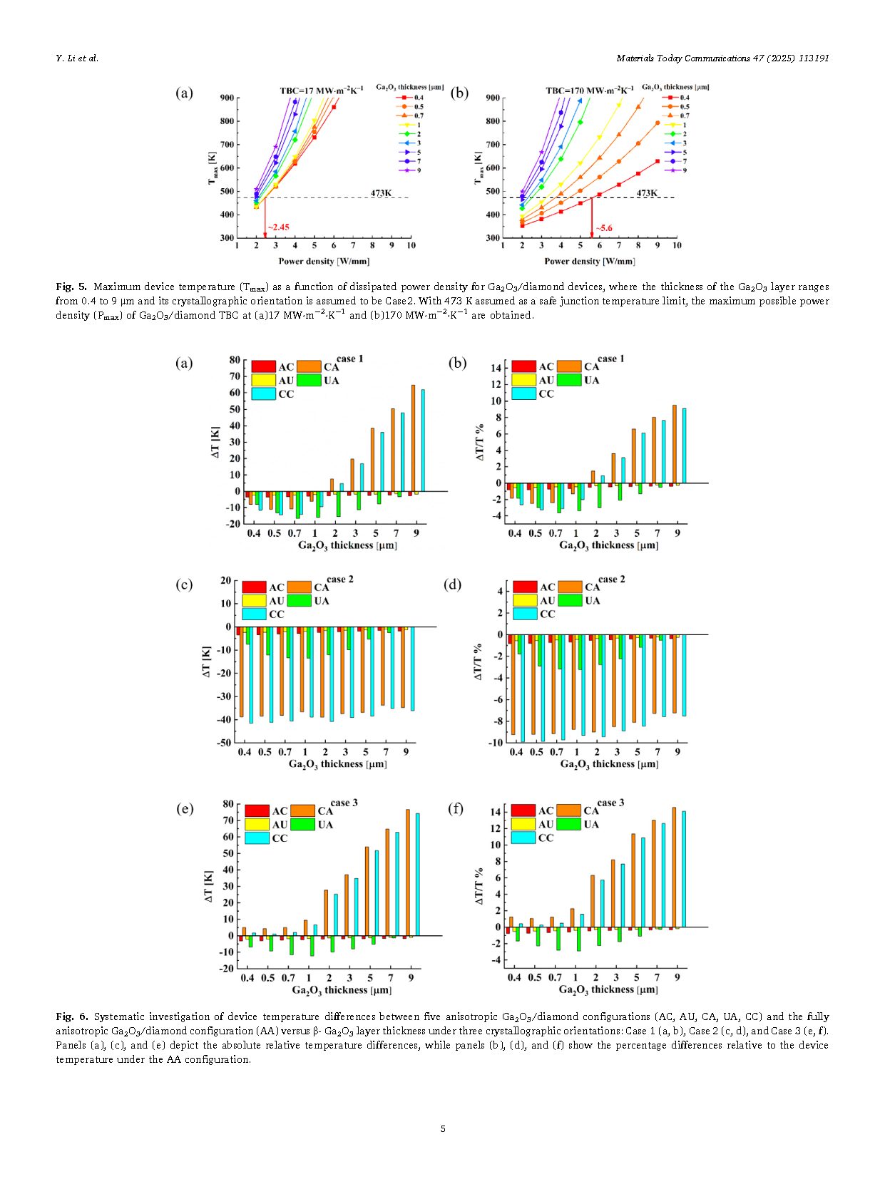
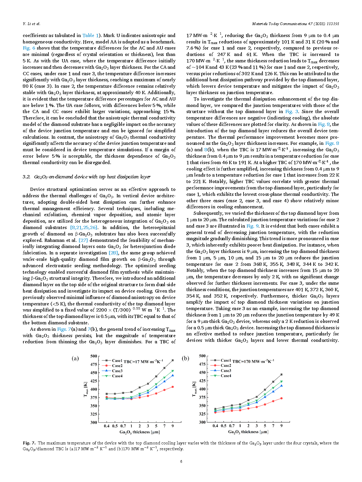
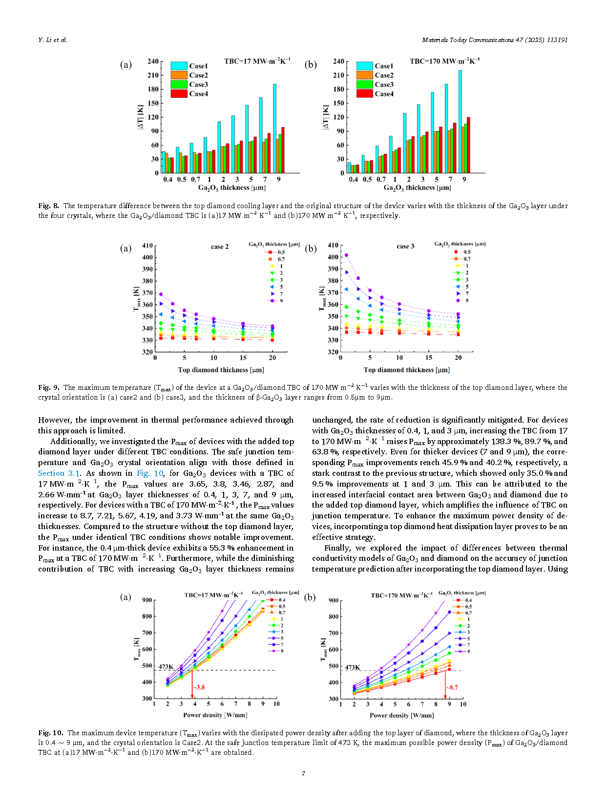
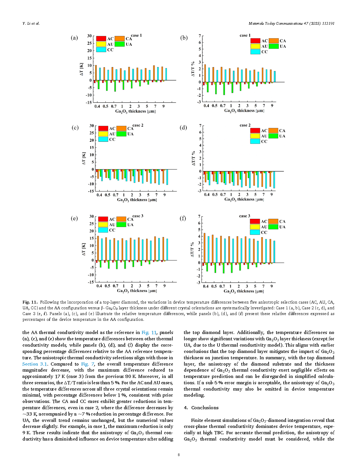
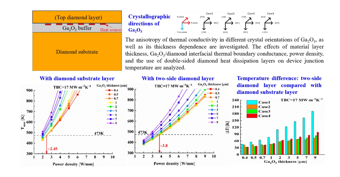
β-Ga2O3 is promising for high-voltage and RF devices but challenged by its low thermal conductivity, causing excessive device temperatures. The integration with high-thermal-conductivity materials like diamond and structure optimization are solutions. However, prior simulations often simplified assumptions on Ga2O3 thickness and bulk thermal conductivity. This work employs 3D finite element thermal analysis to investigate β-Ga2O3-on-diamond cooling strategy, incorporating Ga2O3 and diamond thermal conductivity anisotropy and thickness dependence. We analyze the impact of layer thickness, Ga2O3/diamond interfacial thermal conductance, power density, and double-sided diamond thermal dissipation layers on junction temperature. Results show that Ga2O3 thermal anisotropy is critical for accurate temperature prediction, while diamond anisotropy is negligible. Within a 5 % error margin, the thickness dependence of Ga2O3 thermal conductivity is insignificant with diamond substrate solely, and both the Ga2O3 thickness dependence and its anisotropy can be neglected under double-sided diamond cooling. This study aids thermal management and accurate temperature prediction in Ga2O3/diamond devices.
Conclusions
Finite element simulations of Ga2O3-diamond integration reveal that cross-plane thermal conductivity dominates device temperature, especially at high TBC. For accurate thermal prediction, the anisotropy of Ga2O3 thermal conductivity model must be considered, while the anisotropy of diamond is negligible. Ga2O3 thickness dependence can be ignored within a 5 % error margin. Optimizing crystal orientation and TBC, adding a top diamond layer boosts the maximum power density of a 0.4 μm Ga2O3 device by 55.3 % (to 8.7 W⋅mm-1) versus a substrate-only design. The top diamond’s cooling efficacy increases with higher TBC and lower Ga2O3 cross-plane thermal conductivity. Increasing its thickness further reduces temperature, especially for thicker or lower thermal conductivity Ga2O3 layers (though gains are limited). Crucially, the top diamond mitigates the impact of Ga2O3 thermal conductivity anisotropy and thickness, allowing anisotropy to be neglected within 5 % error.
DOI:
doi.org/10.1016/j.mtcomm.2025.113191