Paper Sharing
【Domestic Papers】Predictive Mobility Model for β-Ga₂O₃ at Cryogenic Temperature
日期:2025-07-04阅读:695
Researchers from the Yanshan University have published a dissertation titled "Predictive Mobility Model for β-Ga₂O₃ at Cryogenic Temperature" in Electronics.
Project Support
This work was supported in part by the National Natural Science Foundation of China under Grant U21A20501 and in part by the Innovation Capability Improvement Project of Hebei Province, China, under Grant 22567605H.
Background
As a representative example of emerging semiconductor materials, gallium oxide (β-Ga₂O₃) exhibits exceptional properties with a wide bandgap of 4.9 eV, a high breakdown field strength of 8 MV/cm, and a Baliga’s Figure of Merit reaching up to 3444 MW/cm2. The listed research results show that β-Ga₂O₃ demonstrates significant potential for use in high-voltage and high-power electronic devices. Compared to materials such as silicon (Si) and gallium nitride (GaN), which have been extensively researched, research on β-Ga₂O₃ is currently still focused on the development of single large-sized crystals and the optimization of device design. Although preliminary results have been obtained for β-Ga₂O₃ in experimental research and application development, in-depth research on the electrical properties of this material, especially regarding mobility models, is not systematic, which limits its application in high-performance electronic devices.
In this paper, the transport characteristics of the carriers in β-Ga₂O₃ and the various scattering mechanisms affecting the carriers were studied. By integrating the impacts of different doping levels and crystal orientations, a β-Ga₂O₃ mobility model was established. Additionally, a series of variable-temperature mobility tests were conducted on Sn-doped n-type (100) and (001) β-Ga₂O₃ using a Hall effect testing system combined with a vacuum deposition technique, covering a temperature range from 15 to 300 K. The exhaustive analysis and fitting of the experimental data yielded models of β-Ga₂O₃ mobility that characterize different crystal orientations and doping levels.
Abstract
In this work, the transport properties of charge carriers in β-Ga₂O₃ were investigated, along with intrinsic physical mechanisms such as lattice vibrations, impurity scattering, and interfacial effects. The high-field behavior of carrier mobility was characterized using vacuum deposition techniques for the fabrication of electrodes with ohmic contacts, and the Hall effect measurement system was employed to test the temperature-dependent mobility of Sn-doped n-type (100) and (001) β-Ga₂O₃ samples at a cryogenic temperature. A predictive model for β-Ga₂O₃ mobility was developed by examining the effects of the temperature on the scattering mechanisms based on a theoretical transport model. The experimental results for β-Ga₂O₃ mobility, which varied with the temperature and doping concentration, showed good agreement with the theoretical model within the temperature range of 15–300 K. The maximum discrepancy between the predictive model and the experimental data was less than 5%. This study provides valuable theoretical insights for the design and simulation of β-Ga₂O₃ devices.
Conclusions
A comprehensive β-Ga₂O₃ mobility test was successfully conducted across an exceptionally broad temperature spectrum. A robust model of gallium oxide mobility was developed after the empirical data were meticulously aligned with a theoretical model of mobility. The relationship between the carrier mobility and temperature is encapsulated in this model, which provides a predictive framework for understanding the behavior of gallium oxide under various thermal conditions.
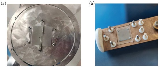
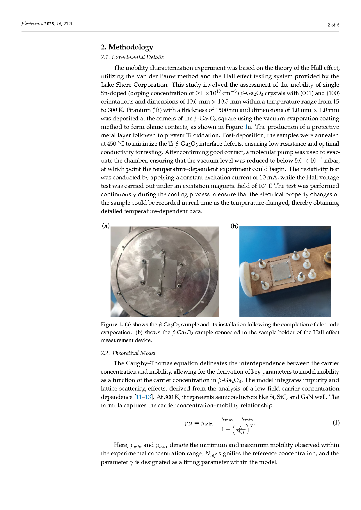
Figure 1. (a) shows the β-Ga₂O₃ sample and its installation following the completion of electrode evaporation. (b) shows the β-Ga₂O₃ sample connected to the sample holder of the Hall effect measurement device.
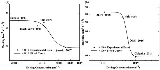
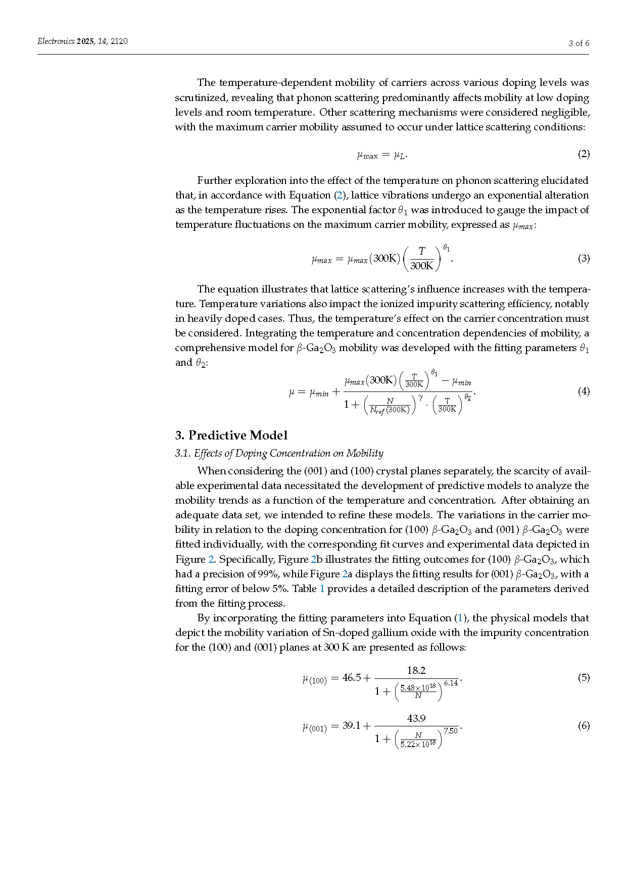
Figure 2. Fitting curves of the mobility–concentration dependence for β-Ga₂O₃. Subfigure (a) illustrates the fitting results for the (001) plane of β-Ga₂O₃, while subfigure (b) depicts the fitting results for the (100) plane.
DOI:
doi.org/10.3390/electronics14112120