Paper Sharing
【Member Papers】Research team from the Southern University of Science and Technology:2.86-kV Vertical Cu₂O/Ga₂O₃ Heterojunction Diodes with Stepped Double-layer Structure
日期:2025-07-08阅读:682
Professors Hongyu Yu and Qing Wang from Southern University of Science and Technology jointly published a paper titled “2.86-kV Vertical Cu2O/Ga2O3 Heterojunction Diodes with Stepped Double-layer Structure” in the Journal of Alloys and Compounds.
Programs
This research was supported by the National Natural Science Foundation of China (NSFC), the Guangdong Provincial Basic and Applied Basic Research Foundation, and the Shenzhen Science and Technology Innovation Commission.
Background
β-Ga2O3 has emerged as a promising candidate for the next generation of high-voltage power devices due to its exceptional breakdown electric field (8 MV/cm), wide bandgap (4.5–4.8 eV), and the feasibility of growing large-sized crystals. However, p-type doping of Ga2O3 is difficult owing to its flat valence band, substantial effective mass, and self-trapped holes, which seriously limit the development of Ga2O3 bipolar power electronics. The alternative solution is to construct all-oxide p-n heterojunction diodes (HJDs) by integrating Ga2O3 with various p-type semiconductors, including Cu2O, NiO and SnO. Cu2O, as a representative p-type oxide semiconductor, offers excellent mobility, thermal stability, and tunable hole concentration, making it a promising material for HJDs applications. However, research on Cu2O/Ga2O3 HJDs remains relatively limited to date.
Research Content
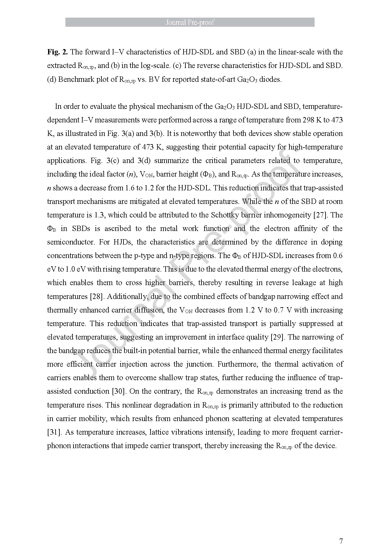
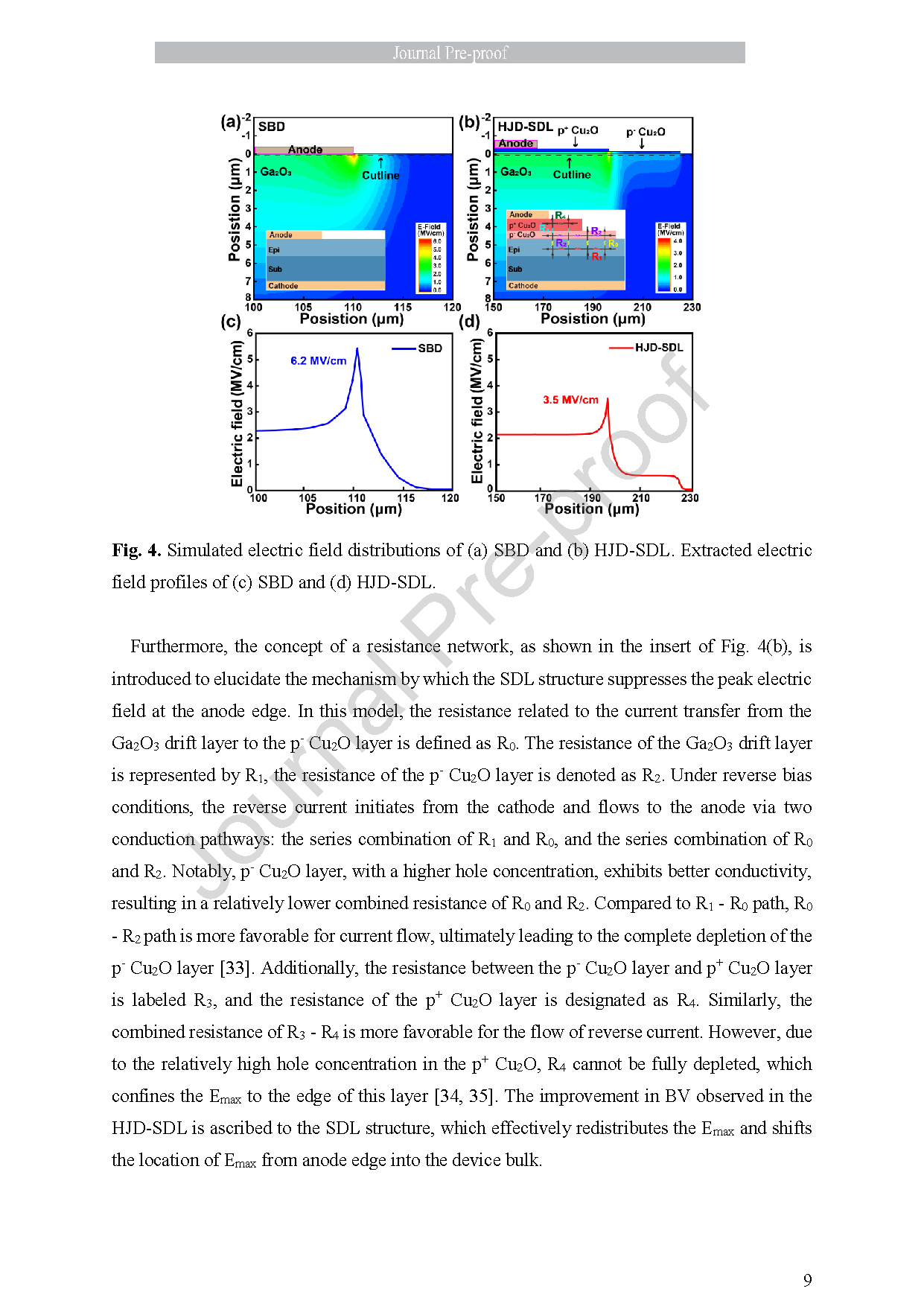
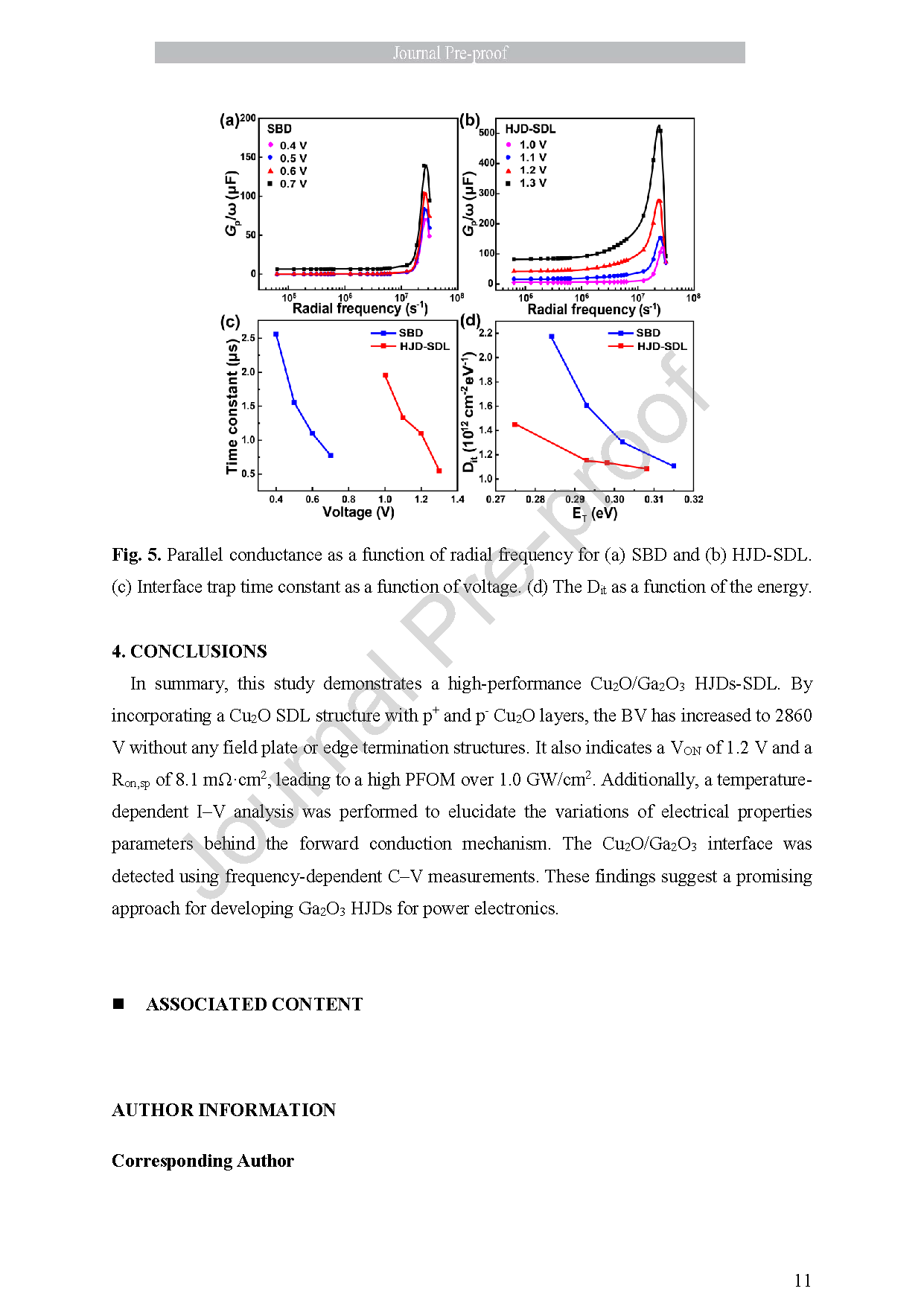
The research team proposed a Cu2O/Ga2O3 HJD with a stepped double-layer structure (HJD-SDL). By modulating the hole concentration gradient across the p⁺/p⁻ Cu2O layers, an optimized electric field distribution within the device was achieved. The device demonstrated a high breakdown voltage of 2.86 kV and a PFOM value of 1.01 GW/cm2. TCAD simulation results demonstrate that the SDL structure effectively suppresses the peak electric field at the anode edge and redistributes it toward the device bulk, thereby enhancing the breakdown voltage capability. The device exhibits stable operation even at elevated temperatures up to 473 K. Temperature-dependent I–V analysis reveals the suppression of trap-assisted transport mechanisms and highlights temperature-induced variations in carrier mobility. Additionally, frequency-dependent capacitance-conductance measurements were conducted to extract the interface trap density. The results confirm that the SDL structure effectively reduces the interface trap density within shallow energy levels, indicating an improved interface quality.
Conclusion
In this study, a Cu2O/Ga2O3 HJDs incorporating SDL structure was successfully fabricated. The device demonstrated an outstanding breakdown voltage of 2.86 kV and a low specific on-resistance of 8.1 mΩ·cm2, achieved without the implementation of any terminal structure. As a result, it exhibited a high PFOM value exceeding 1.0 GW/cm2. These results place this diode at the forefront of currently reported Cu2O/Ga2O3 HJDs. The introduction of the SDL structure not only optimizes the electric field distribution but also enhances the thermal stability and reliability of the device. TCAD simulation results demonstrate that the SDL structure effectively suppresses the peak electric field at the anode edge and redistributes it toward the device bulk, thereby enhancing the breakdown voltage capability. Meanwhile, frequency-dependent capacitance-conductance measurements further confirmed that the SDL structure significantly improves the interface quality of the Cu2O/Ga2O3 HJDs. This study presents a concise and effective heterostructure design strategy, offering both theoretical insights and experimental validation for the development of high-voltage, highly reliable Ga2O3 power electronic devices. The proposed approach shows great promise for advancing future scientific research and industrial applications.
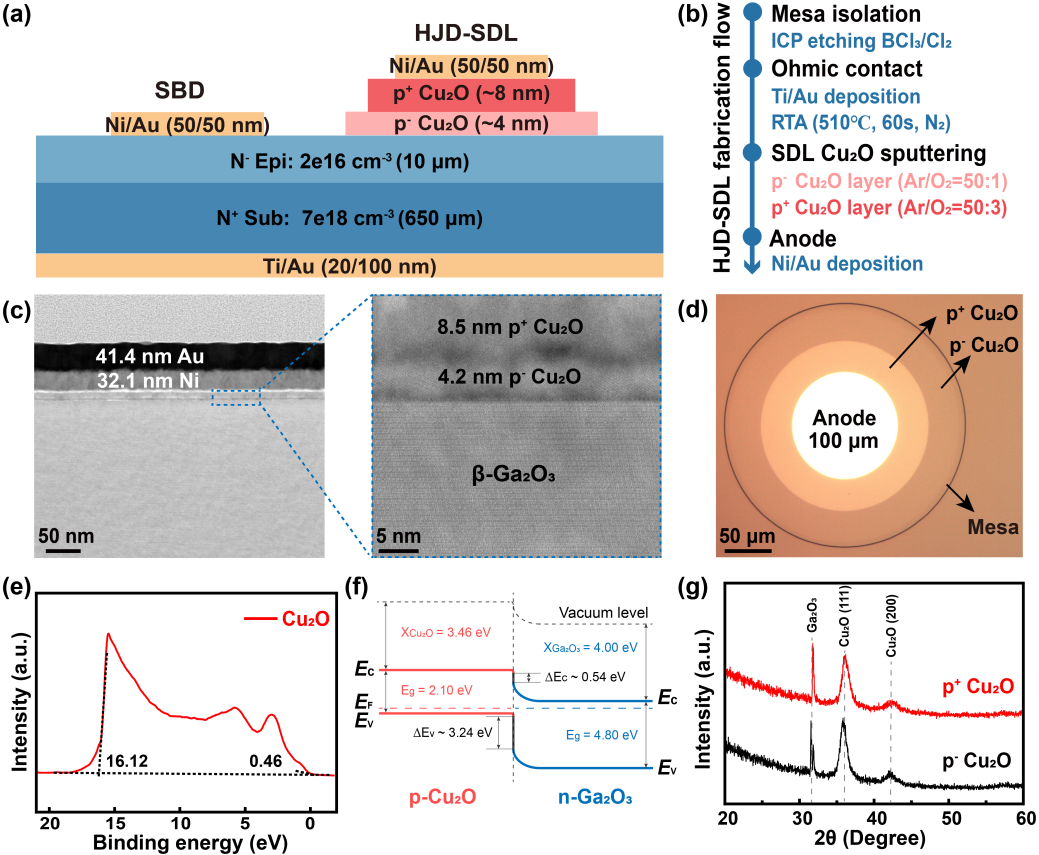
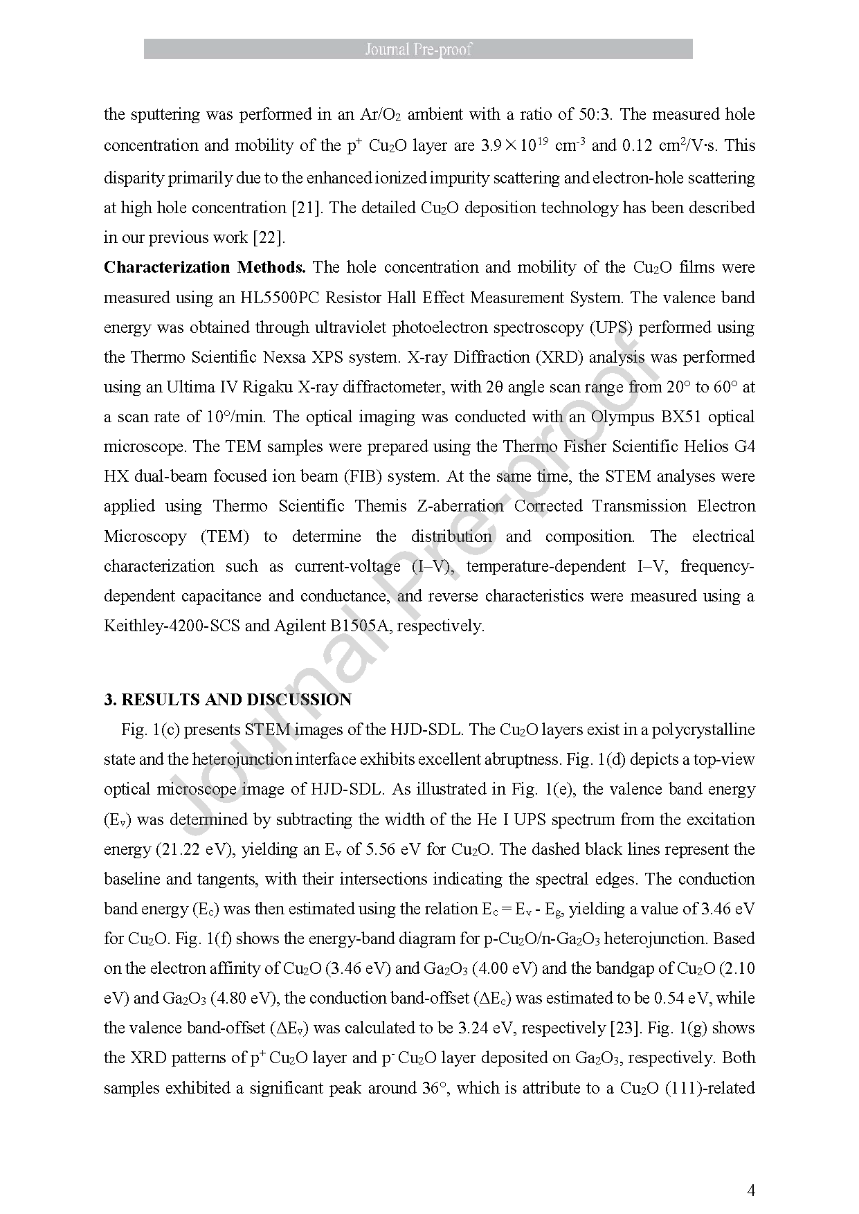
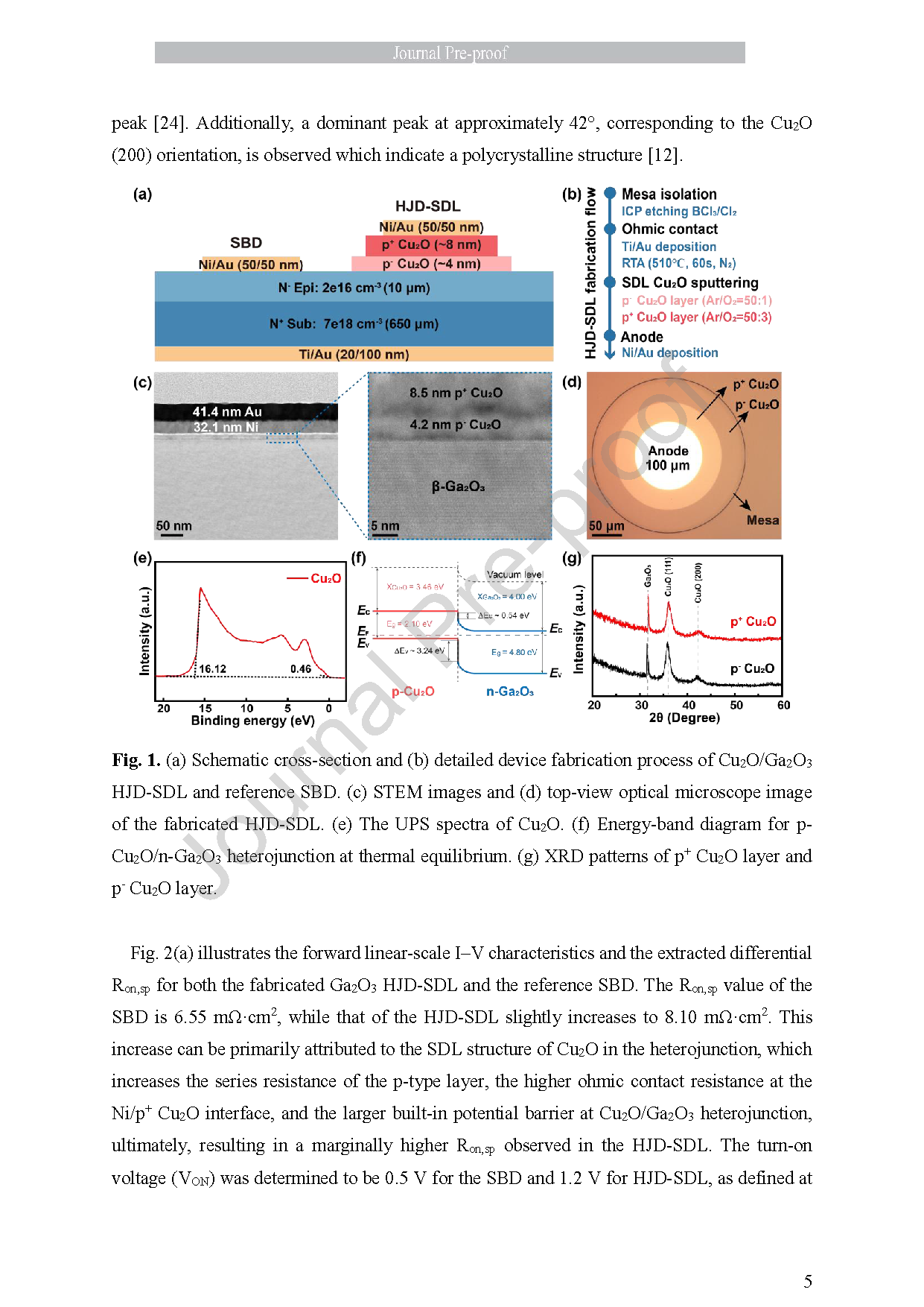
Fig. 1. (a) Schematic cross-section and (b) detailed device fabrication process of Cu2O/Ga2O3 HJD-SDL and reference SBD. (c) STEM images and (d) top-view optical microscope image of the fabricated HJD-SDL. (e) The UPS spectra of Cu2O. (f) Energy-band diagram for p-Cu2O/n-Ga2O3 heterojunction at thermal equilibrium. (g) XRD patterns of p+ Cu2O layer and p- Cu2O layer.
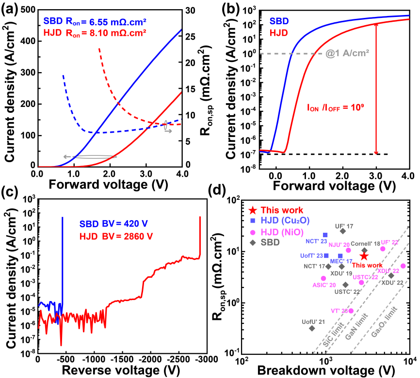
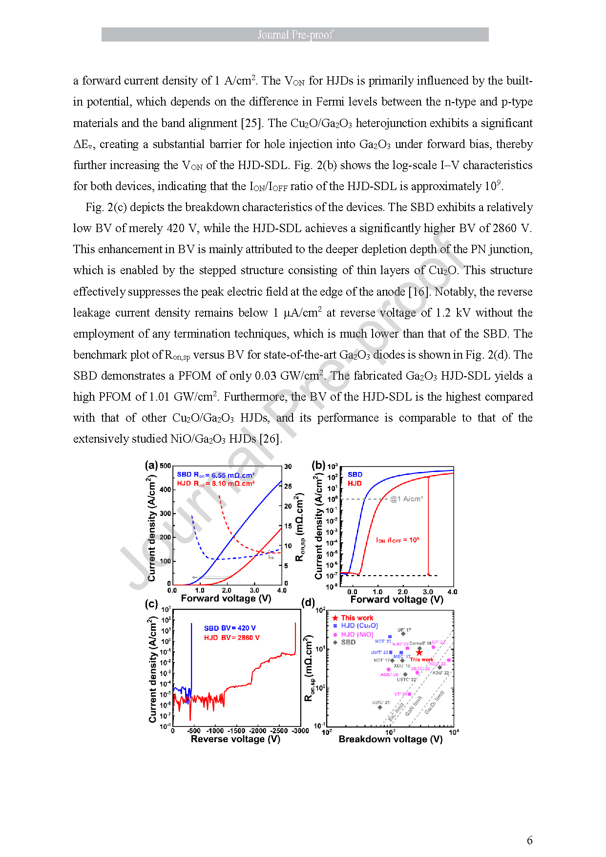
Fig. 2. The forward I–V characteristics of HJD-SDL and SBD (a) in the linear-scale with the extracted Ron,sp, and (b) in the log-scale. (c) The reverse characteristics for HJD-SDL and SBD. (d) Benchmark plot of Ron,sp vs. BV for reported state-of-art Ga2O3 diodes.
DOI:
doi.org/10.1016/j.jallcom.2025.181672