Paper Sharing
【International Papers】Microscopic-scale defect analysis on β-Ga₂O₃ through microscopy
日期:2025-07-08阅读:646
Researchers from the National Institute of Standards and Technology have published a dissertation titled "Microscopic-scale defect analysis on β-Ga2O3 through microscopy" in Applied Physics Letters.
Background
β-phase gallium oxide (β-Ga2O3) is an ultra-wide bandgap material with a bandgap of 4.8 eV and a corresponding large breakdown electric field of ~8MV cm-1 and Baliga’s figure of merit of approximately 2870.7 Due to the availability of large, high-quality substrates grown from melt, β-Ga2O3 has potential cost savings over SiC and GaN technologies in high-power applications. β-Ga2O3 has begun rapid device development; however, several material issues need to be addressed. In SiC, killer defects, such as micro pipes, stacking faults, and processing damage, were crucial to be eliminated for commercial devices, while threading dislocations and stacking faults in GaN have been correlated with device leakage and reliability. Similar issues may also affect β-Ga2O3, and several common defects in bulk substrates grown via edge-defined film-fed growth and vertical Bridgeman methods have been identified and classified. Nanovoid defects have been frequently observed and are correlated with leakage current, possibly due to forming threading dislocations, in Schottky barrier diodes (SBDs). Other types of dislocations have been observed in β-Ga2O3, and some are associated with leakage current in SBDs though it is often challenging to identify the exact dislocation type.
Abstract
β-Ga2O3 is a wide bandgap semiconductor with potential for surpassing current-generation high-power device performance and cost-effectiveness, due to its unique properties and availability of large high-quality substrates. However, β-Ga2O3 power electronics are still relatively immature, and commercial realization of reliable high-power devices will require intimate knowledge of performance-limiting extended defects. While several defects have been characterized in bulk substrates, less attention has been given to defects in homoepitaxially grown β-Ga2O3, despite its importance in producing high quality active layers for power devices. In this work, we characterize the bulk electronic properties and extended structural defects in (010) β-Ga2O3 homoepitaxially grown via hydride vapor phase epitaxy (HVPE) using photoemission, transmission electron microscopy (TEM), and complementary spectroscopy and microscopy techniques. We observe two types of linear, surface defects aligned along the [001] crystal axis. One defect consists of a micrometer-sized particle and a tail of protruding material, while the other is a groove in the surface. The large particle is a Ga-rich phase that is likely present early in the HVPE growth that disrupts the surface, while the groove defect appears purely structural in nature. Defect etching and TEM analysis reveal that the linear defects are associated with different dislocation structures, which can explain the different local conductivity measured at each. Our results emphasize that proper surface processing of the bulk substrate is still necessary for obtaining higher quality epitaxial growth for large area power devices.
Conclusion
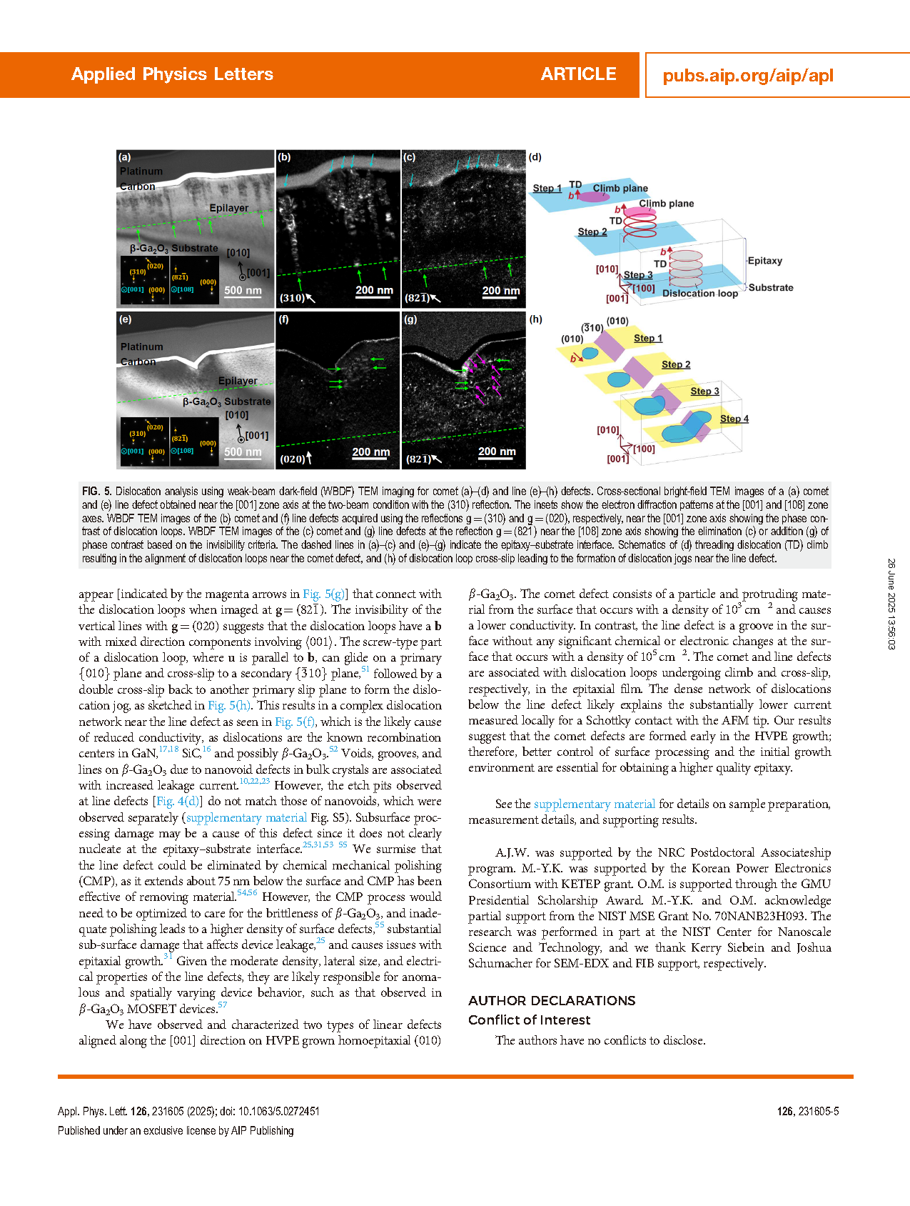
We have observed and characterized two types of linear defects aligned along the [001] direction on HVPE grown homoepitaxial (010) β-Ga2O3. The comet defect consists of a particle and protruding material from the surface that occurs with a density of 103 cm-2 and causes a lower conductivity. In contrast, the line defect is a groove in the surface without any significant chemical or electronic changes at the surface that occurs with a density of 105 cm-2. The comet and line defects are associated with dislocation loops undergoing climb and cross-slip, respectively, in the epitaxial film. The dense network of dislocations below the line defect likely explains the substantially lower current measured locally for a Schottky contact with the AFM tip. Our results suggest that the comet defects are formed early in the HVPE growth; therefore, better control of surface processing and the initial growth environment are essential for obtaining a higher quality epitaxy.

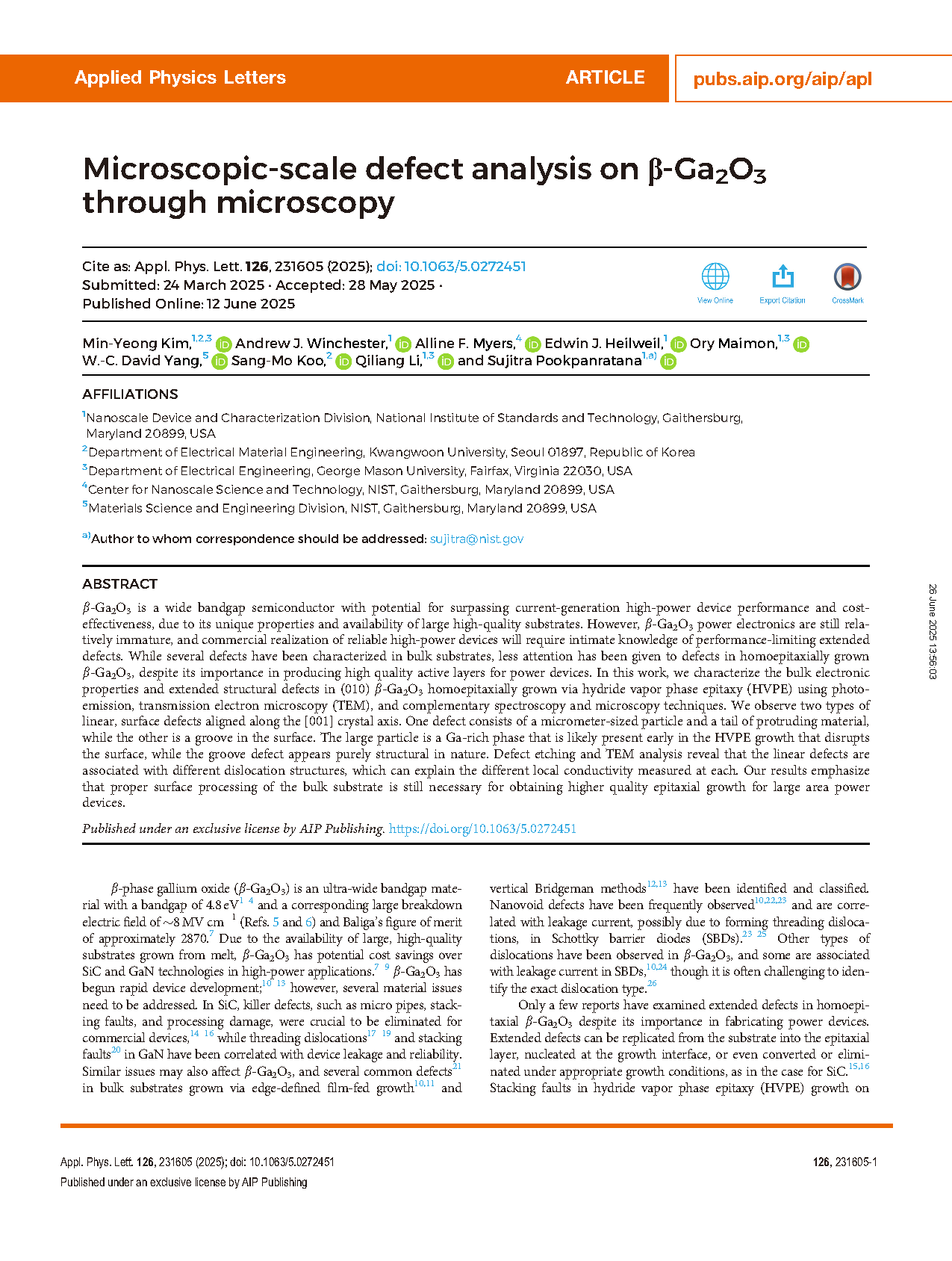
FIG. 1. PES measurements of (a) the secondary electron cutoff and the valence band edge of the epitaxial β-Ga2O3 using (b) He I and (c) and (d) Al Kα excitations. The valence bands in (b) and (c) are in linear scale, while (d) and inset of (b) are on semi-log scales. The red lines are linear fits of the data.
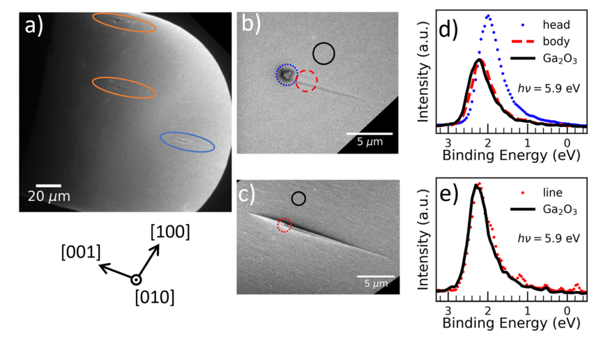
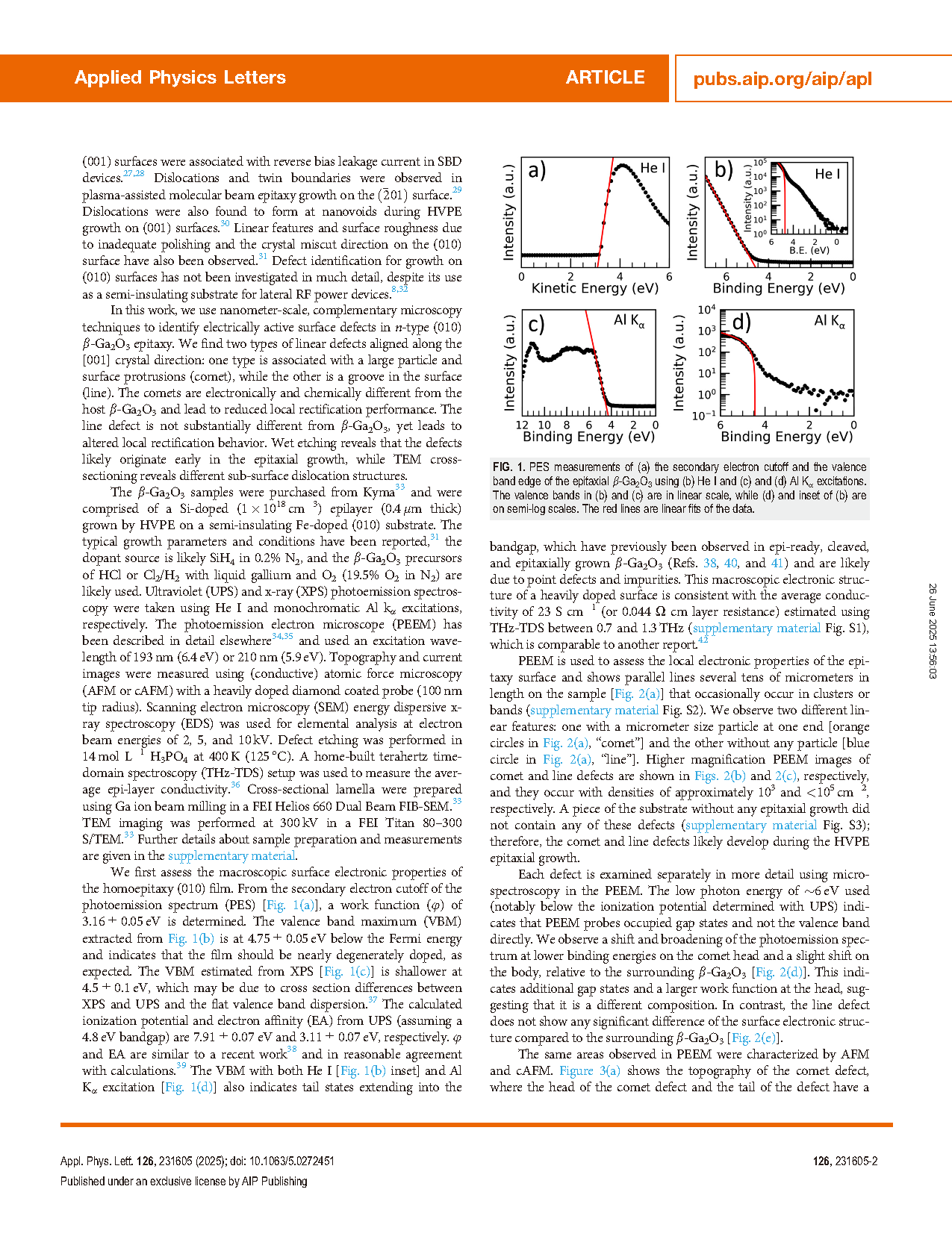
FIG. 2. PEEM observations of (a) comet and line defects circled in orange and blue, respectively, and at a higher magnification at (b) a comet and (c) a line defect. PEEM PES spectrum from the areas marked by solid and dashed circles in (b) and (c) for (d) a comet defect and (e) a line defect, respectively. For (d) and (e), the work function measured with He I UPS was used to convert to an approximate binding energy scale.
DOI:
doi.org/10.1063/5.0272451