Paper Sharing
【International Papers】>3kV NiO/Ga₂O₃ Heterojunction Diodes With Space-Modulated Junction Termination Extension and Sub-1V Turn-On
日期:2025-07-08阅读:682
Researchers from the Arizona State University have published a dissertation titled ">3kV NiO/Ga2O3 Heterojunction Diodes With Space-Modulated Junction Termination Extension and Sub-1V Turn-On" in IEEE Journal of the Electron Devices Society.
Background
Over the past decade, β-Ga2O3 has emerged as a prime candidate for next generation power electronics, owing to the high critical electric field (8 MV/cm), ease of n-type doping, and availability of large-area single crystal substrates. The availability of high quality, low defect density β-Ga2O3 drift-layers grown on bulk β-Ga2O3 substrates coupled with advanced damage-free etching techniques are paving the way for high-performance Ga2O3 power devices. In particular, two-terminal vertical β-Ga2O3 devices have shown great improvements in performance over the past few years, exceeding the unipolar FOM of both SiC and GaN. Majority of these reports employ p-NiO/Ga2O3 heterojunctions that have demonstrated superior breakdown performance. However, a key limitation with these HJDs is the much larger turn on voltage (VON) of ~2V. A higher VON results in significantly higher conduction losses (~ION2 VF, where VF=VON+ ION× Ron,sp), degrading device efficiency. Therefore, achieving high breakdown voltage while maintaining low VON is critical for enabling low-loss β-Ga2O3 rectifiers.
Abstract
This work demonstrates high-performance vertical NiO/Ga2O3 heterojunction diodes (HJDs) with a 2-step space-modulated junction termination extension. Distinct from the current state-of-the-art Ga2O3 HJDs, we achieve breakdown voltage exceeding 3 kV with a low turn on voltage (VON) of 0.8V, estimated at a forward current density (IF) of 1 A−cm-2. The measured devices exhibit excellent turn-on characteristics achieving 100 A−cm-2 current density at a forward bias of 1.5 V along with a low differential specific on-resistance (Ron,sp) of 4.4 m Ω -cm2. The SM-JTE was realized using concentric NiO rings with varying widths and spacing that approximates a gradual reduction in JTE charge. The unipolar figure of merit (FOM) calculated exceeds 2 GW-cm2 and is among the best reported for devices with a sub-1V turn-on. The fabricated devices also displayed minimal change in forward I-V characteristics post reverse bias stress of 3 kV applied during breakdown voltage testing.
Conclusion
In conclusion, we demonstrate p-NiO/Ga2O3 HJDs with space-modulated junction termination extension (SM-JTE) enabling a gradual reduction in JTE charge. We simultaneously obtain excellent forward and reverse performance including a low VON of 0.8 V, VBR of 3 kV and Ron of 4.4 mΩ -cm-2 resulting in a power figure of merit exceeding 2 GW-cm-2. We also report a record low effective Ron of 14.5mΩ-cm-2 for NiO/Ga2O3 HJDs. The high-voltage reverse blocking capacity with sub-1V turn-on voltage showcases the great promise of Ga2O3 HJDs for low-loss kilovolt class power electronics.
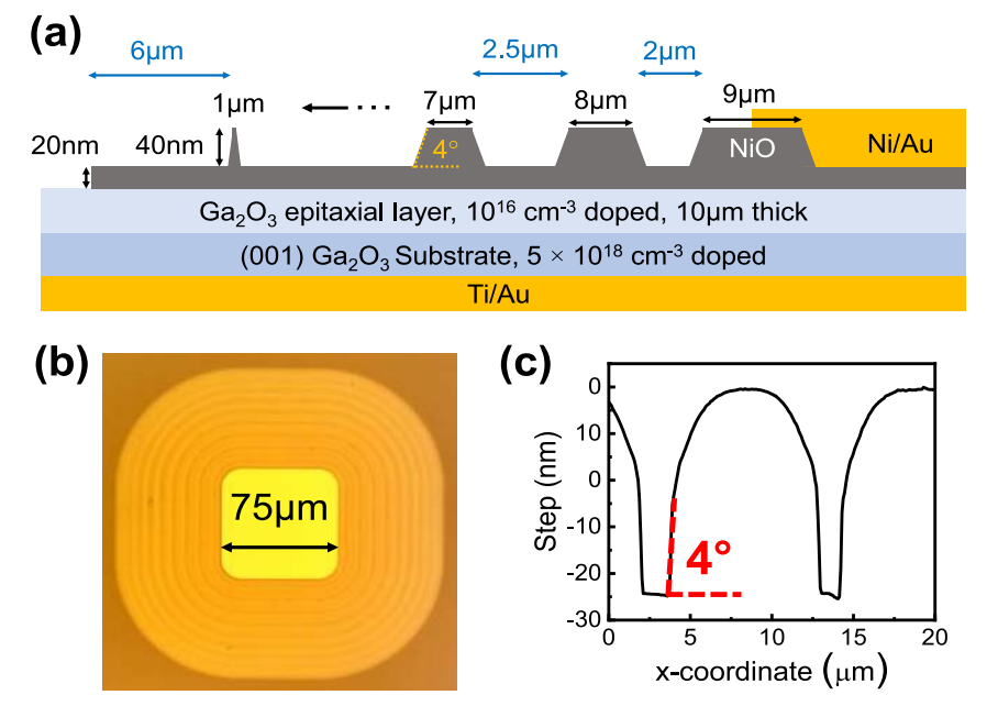
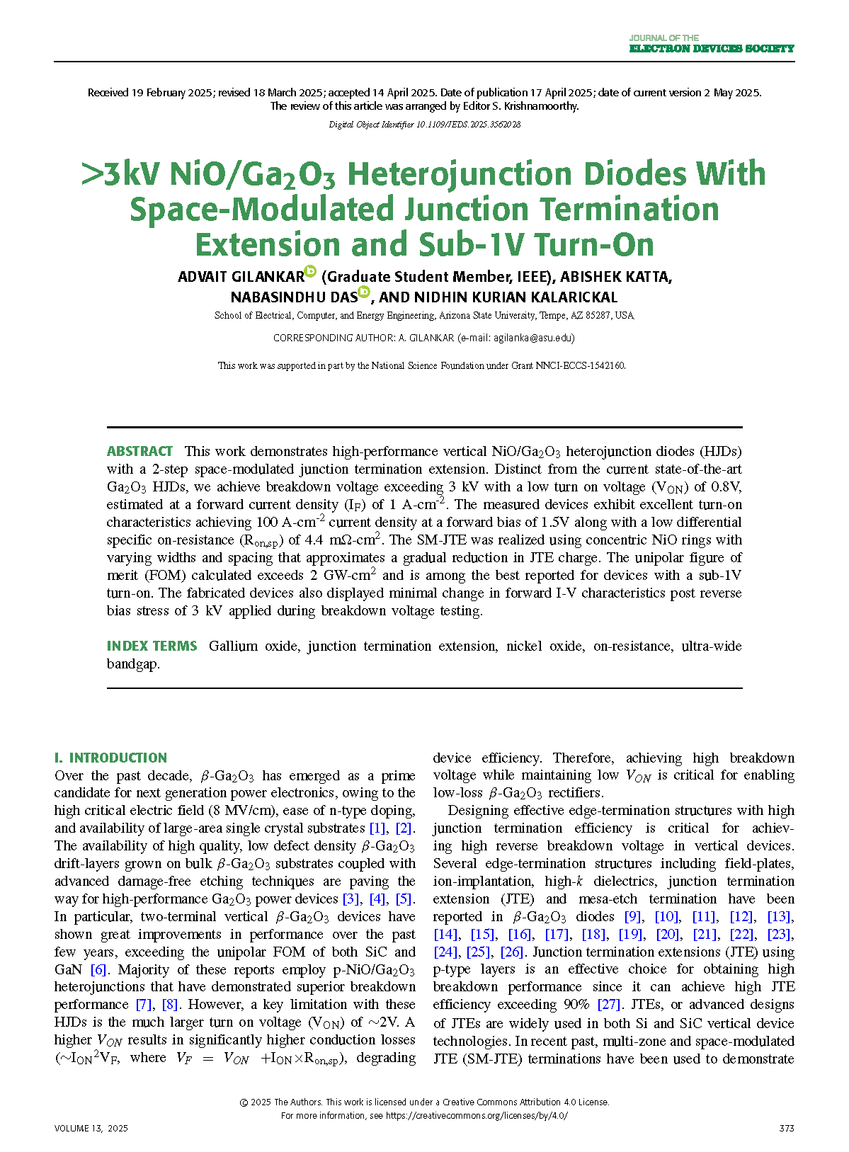
FIGURE 1. (a) Cross-section schematic of fabricated p-NiO/Ga2O3 diode with SM-JTE termination. (b) Top-view optical image of fabricated 75μ m active area device. (c) AFM Scan across the JTE structure showing a bevel angle of ~4° for NiO JTE rings.
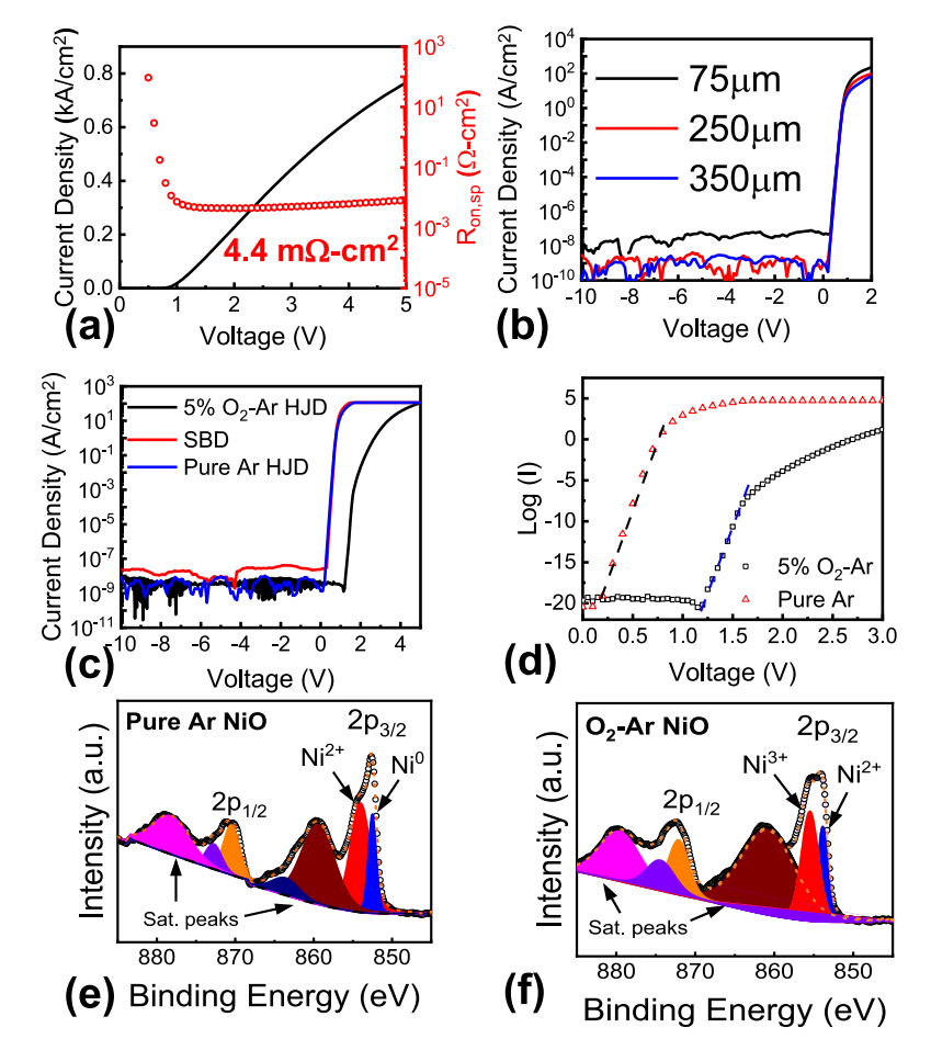
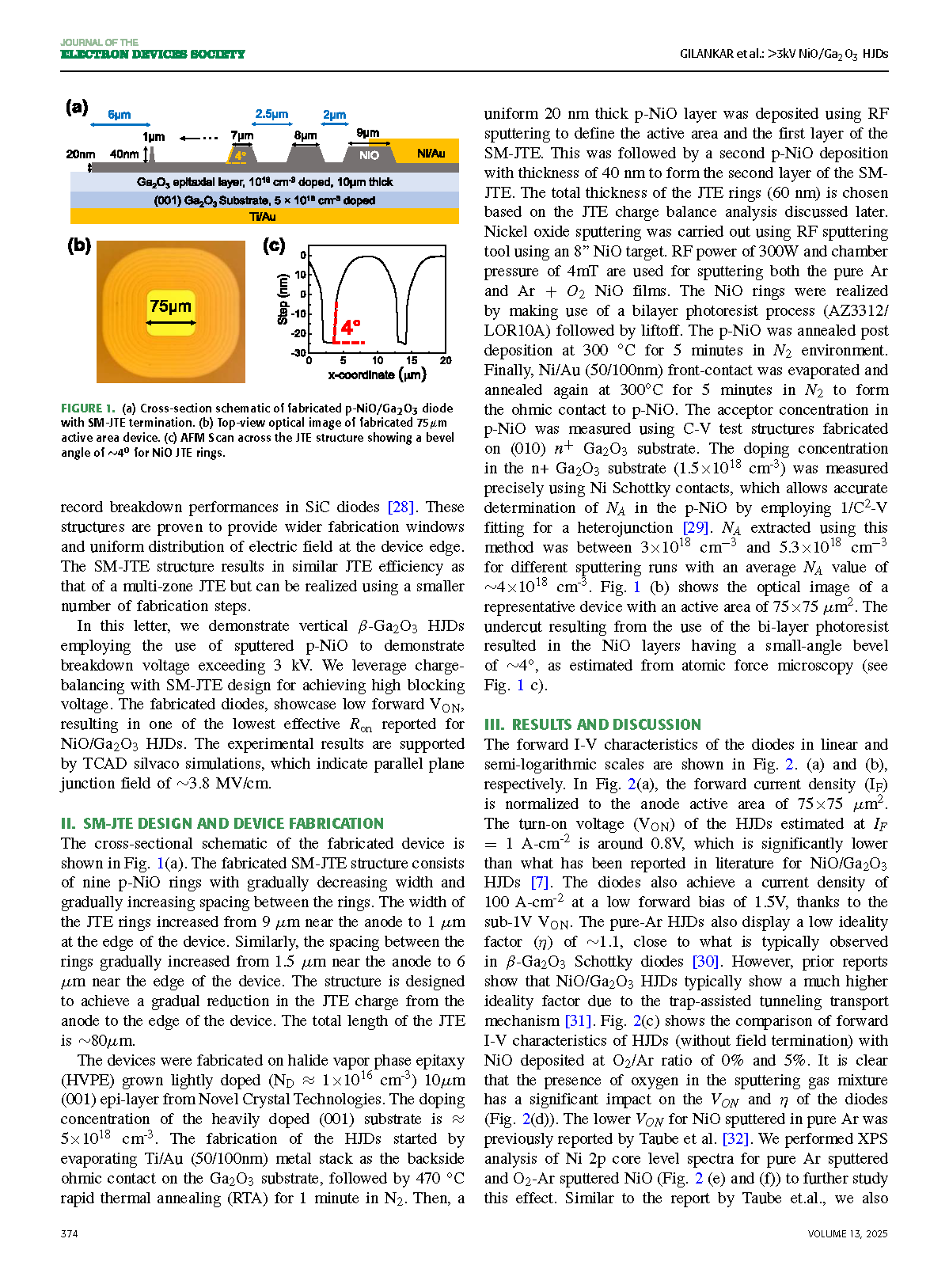
FIGURE 2. (a) Forward I-V characteristics in linear scale and differential specific on-resistance for 75μ m area device. (b) Forward I-V characteristics in semi-log scale for devices with 3 different active areas. (c) Forward I-V characteristics plotted in semi-log scale for SBD, pure-Ar sputtered NiO/Ga2O3 diode and 5%O2-Ar sputtered NiO/Ga2O3 diodes. (d) Ideality factor extraction from semi-log I-V plot for pure-Ar and 5% O2-Ar sputtered NiO/Ga2O3 diode. Ni 2p core level scans for sputtered NiO in (e) pure-Ar atmosphere (f) O2-Ar atmosphere.
DOI:
doi.org/10.1109/JEDS.2025.3562028