Paper Sharing
【Domestic Papers】 High-Performance Ultraviolet Photodetectors Based on Ga₂O₃/GaN Gradient Heterojunction
日期:2025-07-08阅读:670
Researchers from the Songshan Lake Materials Laboratory & Dongguan University of Technology have published a dissertation titled "High-Performance Ultraviolet Photodetectors Based on Ga2O3/GaN Gradient Heterojunction" in IEEE Transactions on Electron Devices.
Background
Gallium nitride (GaN)-based ultraviolet (UV) photodetectors (PDs) have drawn extensive attention due to their excellent radiation resistance, high UV–visible rejection ratio, and potential applications in UV curing, environmental monitoring, missile warning, and other fields. Although commercial GaN single-crystal films exhibit high crystallinity, their optoelectronic performance is limited by inefficient carriers’ separation and significant charge mobility disparity (a hole mobility of 150 cm2/V·s and an electron mobility of 1000 cm2/V·s). The absence of built-in electric fields further exacerbates electron–hole recombination probabilities, reducing the responsivity of PDs. To improve the responsivity of GaN PDs, significant efforts have been made, including defect control, transparent electrodes, surface treatment, and heterojunction construction.
Project Support
This work was supported in part by the National Natural Science Foundation of China under Grant 62204039 and in part by the “Innovative and Strengthen University” Program of Department of Education of Guangdong Province under Grant 2023KSYS003.
Abstract
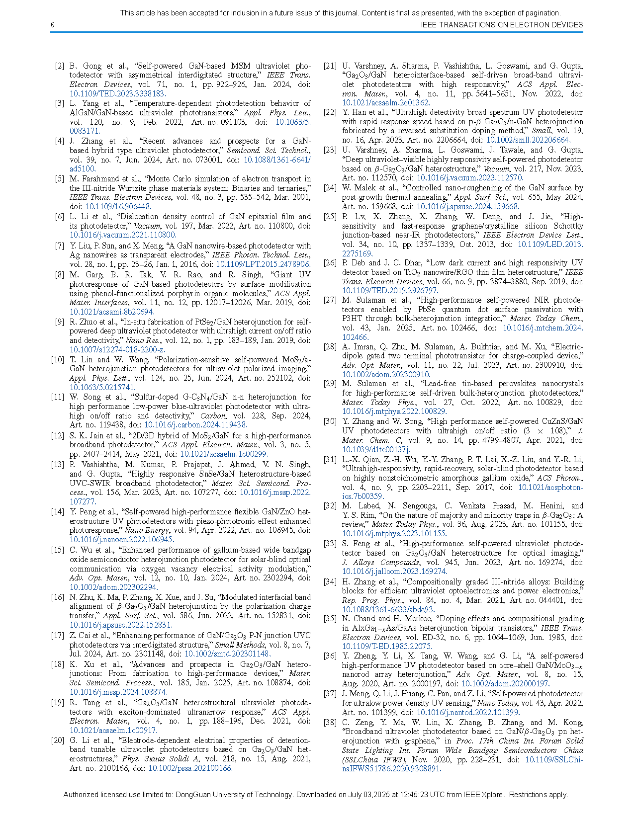
Gallium nitride (GaN)-based ultraviolet (UV) photodetectors (PDs) have attracted widespread attention due to their potential applications in UV curing, environmental monitoring, and other fields. However, the GaN PDs generally exhibit low responsivity due to poor carriers’ separation efficiency. Gallium oxide (Ga2O3)/GaN heterostructure is an ideal material for fabricating high-performance UV PDs due to appropriate bandgap and differences in energy band. In this regard, we have demonstrated the Ga2O3/GaN gradient heterostructure UV PDs with high photoresponse performance. The Ga2O3 layer was prepared by magnetron sputtering combined with thermal annealing (TA). TA promotes not only the crystalline quality of the Ga2O3 layer but also the transformation of abrupt Ga2O3/GaN heterojunctions into gradient Ga2O3/GaN heterojunctions. The as-fabricated Ga2O3/GaN heterostructure UV PD exhibits a high responsivity of 178.9 (254 nm) and 213.3 A/W (365 nm), with the corresponding detectivity of 3.0 × 10¹⁵ and 3.6 × 10¹⁵ Jones. This work provides a promising pathway toward UV PDs with a high responsivity range from UV-A to UV-C bands.
Conclusion
In conclusion, Ga2O3/GaN heterojunction UV PDs with high responsivity and detectivity can be achieved by combining the magnetron sputtering growth of Ga2O3 with TA. At a bias voltage of 5 V, the responsivity of as-deposited PDA is 6.7 A/W at 254 nm (140 µW/cm2) and 18.7 A/W at 365 nm (50 µW/cm2), and the detectivity of 3.5×10¹³ Jones (254 nm) and 9.6 × 10¹³ Jones (365 nm). Different from PD-A, the Ga2O3 layer transforms from amorphous to polycrystalline through TA, resulting in a significant improvement in crystal quality; on the other hand, the gradient Ga2O3/GaN heterojunction can be formed by thermal diffusion of N and O elements at the interface, which effectively improves the separation efficiency of photogenerated charge carriers. Based on the above reasons, both the responsivity and detectivity of PD-B are one order of magnitude higher than PD-A under a bias voltage of 5 V. Under 254- and 365-nm UV radiation, the responsivity of PD-B is 178.9 and 213.3 A/W, respectively, with the corresponding detectivity of 3.0 × 10¹⁵ Jones and 3.6 × 10¹⁵ Jones. Specifically, both PD-A and PD-B exhibit higher photoresponse to UV radiation than PD-C, which further confirms that Ga2O3/GaN heterojunction can enhance the separation efficiency of photogenerated carriers, thereby improving the performance of the PD.
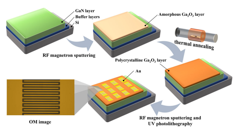
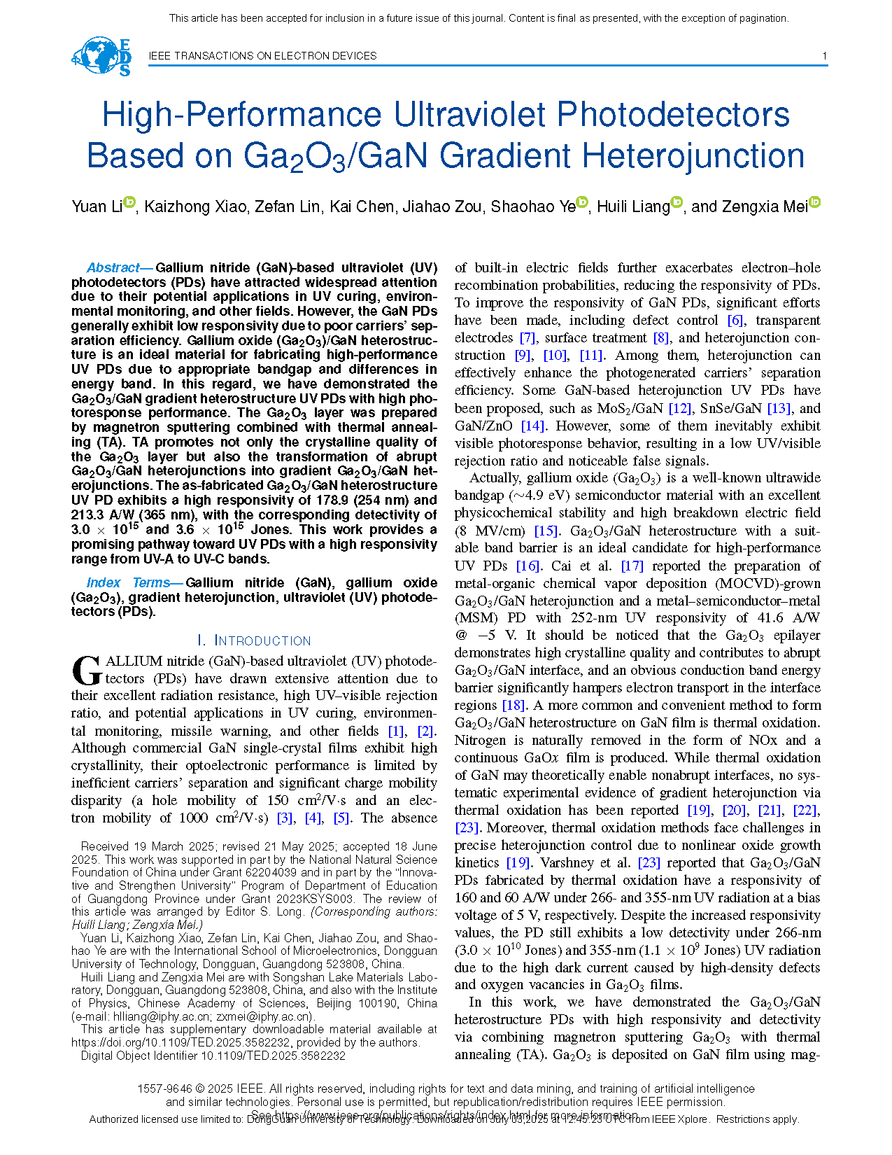
Fig. 1. Schematic of Ga2O3/GaN heterojunction growth and MSM UV PD fabrication.
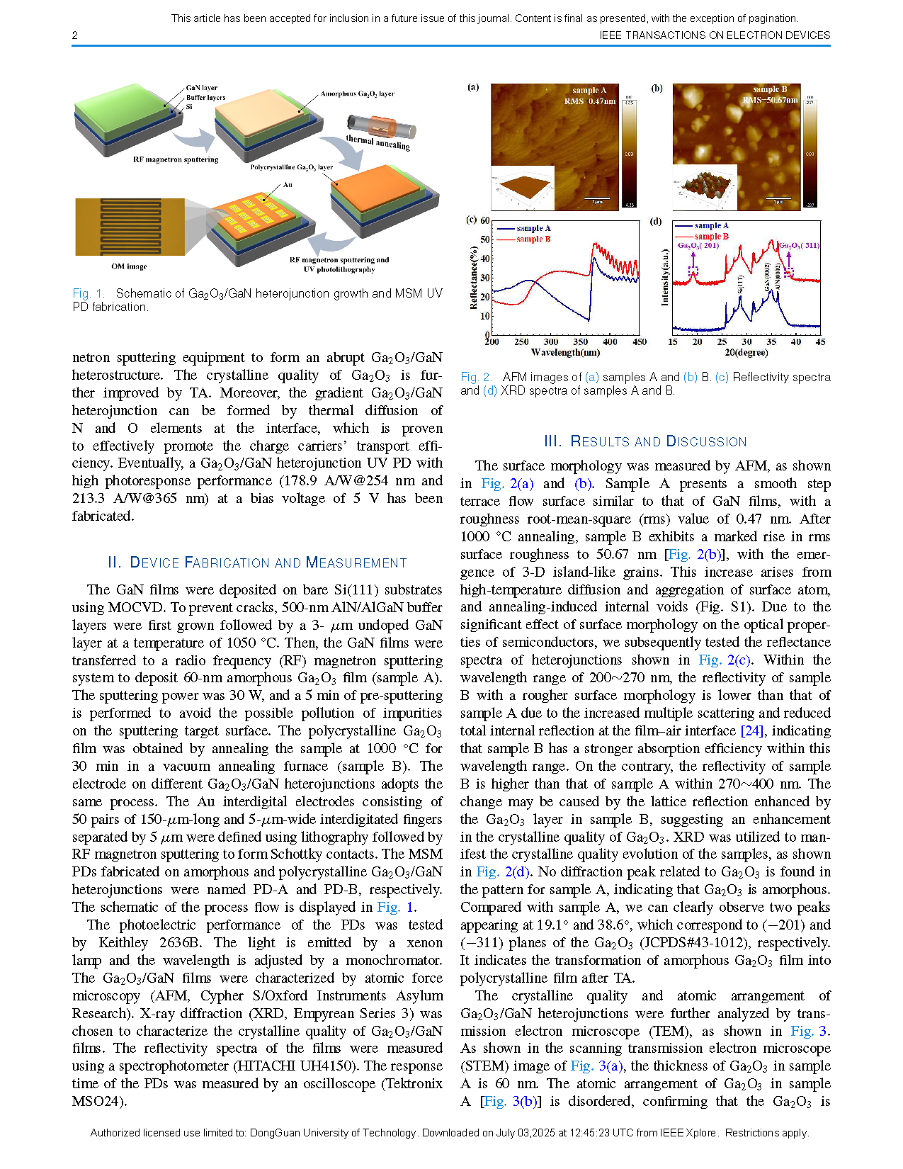
Fig. 2. AFM images of (a) samples A and (b) B. (c) Reflectivity spectra and (d) XRD spectra of samples A and B.
DOI:
doi.org/10.1109/TED.2025.3582232