Paper Sharing
【International Papers】Comparative Study on Transient Thermal Resistance for β-Ga₂O₃ SBDs with Junction-Side Cooling Implementation
日期:2025-07-10阅读:635
Researchers from the Osaka University have published a dissertation titled "Comparative Study on Transient Thermal Resistance for β-Ga2O3 SBDs with Junction-Side Cooling Implementation" in ISPSD 2025.
Background
Gallium oxide (Ga2O3) semiconductors have emerged as a highly promising material for next-generation power electronics systems due to their ultra-wide bandgap, high critical electric field, and excellent thermal stability. These unique properties make Ga2O3-based devices highly suitable for applications in high-voltage and high-power systems beyond the silicon carbide (SiC) and gallium nitride (GaN) power semiconductor devices. Several teams have reported Ga2O3 Schottky barrier diodes (SBDs) and metal-oxide-semiconductor field effect transistors (MOSFETs). Note that Ga2O3 has several polymorphic structures such as α- and β-types, and β-type Ga2O3 is often studied as power devices because it is easy to grow its single crystal by melting it at atmospheric pressure.
Abstract
Ga2O3 power semiconductor devices have promising superior performance beyond SiC and GaN power semiconductor devices for future HV applications. However, their thermal management is important because they have low thermal conductivity compared to Si and SiC, which could be a disadvantage to utilizing them for practical applications. This paper evaluates the effectiveness of the junction-side cooling implementation for reducing the transient thermal resistance of Ga2O3 SBDs.
Conclusion
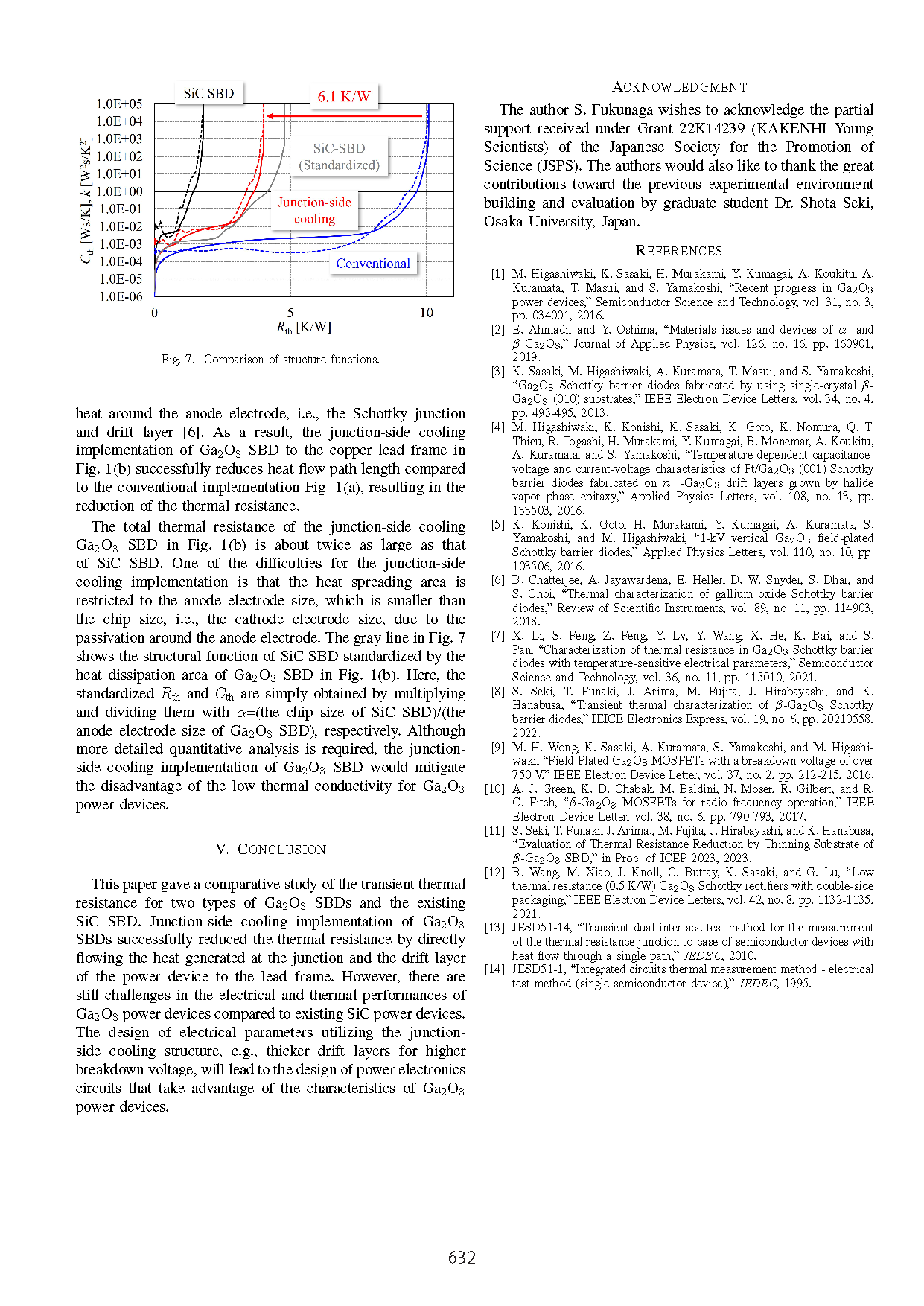
This paper gave a comparative study of the transient thermal resistance for two types of Ga2O3 SBDs and the existing SiC SBD. Junction-side cooling implementation of Ga2O3 SBDs successfully reduced the thermal resistance by directly flowing the heat generated at the junction and the drift layer of the power device to the lead frame. However, there are still challenges in the electrical and thermal performances of Ga2O3 power devices compared to existing SiC power devices. The design of electrical parameters utilizing the junctionside cooling structure, e.g., thicker drift layers for higher breakdown voltage, will lead to the design of power electronics circuits that take advantage of the characteristics of Ga2O3 power devices.
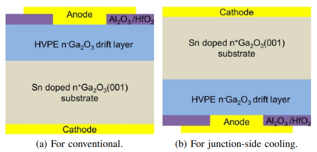
Fig. 1. Corss-sectional structures of studied Ga2O3 SBD bare dies. The bottom side of the figure is soldered to a lead frame.
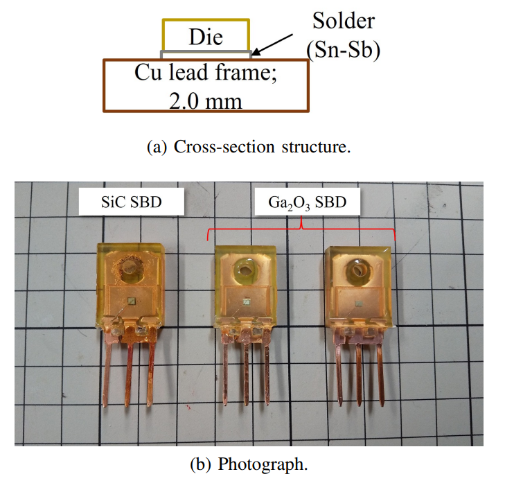
Fig. 2. Studied SBD samples.