Paper Sharing
【Member Papers】Synthesis and characterization of β-Ga₂O₃ nanowires on 4H-SiC substrates via Au-catalyzed low-pressure chemical vapor deposition
日期:2025-07-10阅读:712
Researchers from the Xi’an University of Technology have published a dissertation titled "Synthesis and characterization of β-Ga2O3 nanowires on 4H-SiC substrates via Au-catalyzed low-pressure chemical vapor deposition" in Journal of Crystal Growth.
Project Support
This work was supported by the National Natural Science Foundation of China (Grant No. 62474139, 62404180 and 62104186); Science and technology planning project of Xi’an (No. 2023JH-GXRC-0122); Natural Science Basic Research Plan in Shaanxi Province under Program (Grant 2023-JC-QN-0735); Shaanxi innovation capability support project (Grant No. 2022TD-39). Key Research and Development Project of Shaanxi Province (2023-YBGY-191).
Background
As an ultra-wide bandgap semiconductor with a bandgap of 4.9 eV, β-Ga2O3 has emerged as a highly promising candidate material for solar-blind ultraviolet photodetectors. To transcend the inherent limitations of conventional thin-film devices, one-dimensional Ga2O3 nanostructures exhibiting enhanced surface-to-volume ratios and quantum confinement effects have emerged as focal points of contemporary research. Meitei et al. successfully fabricated β-Ga2O3 nanowire photodetectors utilizing Ag-assisted glancing angle deposition (GLAD) methodology, demonstrating exceptional temporal response characteristics (τr/τd = 0.23 s/0.41 s). These results substantiate the pivotal role of nanowire morphologies in modulating carrier transport dynamics. β-Ga2O3 nanorod arrays synthesized on p-GaN substrates via hydrothermal techniques exhibited significant optoelectronic performance metrics, including a responsivity of 1.19 × 10⁻¹ A/W and photosensitivity of 730.7 % under 260 nm illumination.
Abstract
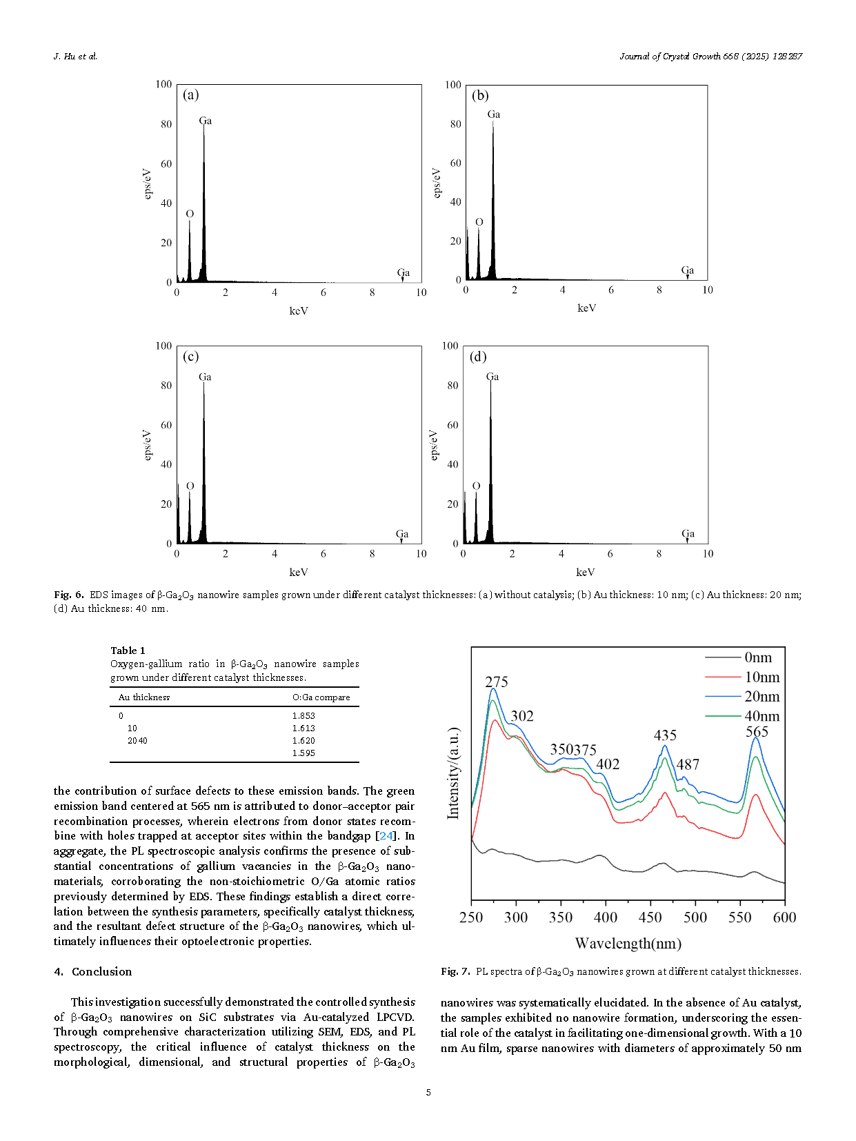
In this paper, we synthesized β-Ga2O3 nanowires on 4H-SiC substrates via Low-Pressure Chemical Vapor Deposition (LPCVD) with Au as a catalyst. Au nanofilms of varying thicknesses (0–40 nm) were sputtered onto 4H-SiC substrates, followed by thermal treatment at 1000 °C. The morphological characteristics of the resultant β-Ga2O3 nanowires were systematically examined as a function of Au nanofilm thickness, facilitating a comprehensive analysis of the underlying growth mechanisms. The study elucidated the correlation between catalyst film thickness and nanowire formation dynamics during LPCVD synthesis. Results demonstrated that decreasing Au nanofilm thickness corresponds to β-Ga2O3 nanowires with reduced diameters, while simultaneously inhibiting the formation of columnar and lamellar nanostructures.
Highlights
· Grow β-Ga2O3nanowires on 4H-SiC substrates via the LPCVD.
· Study effects of Au-catalyst on properties of the nanowires.
· Demonstrate growth mechanism transition from VLS-dominated to hybrid VLS-VS as Au film thickens.
· Identify 10-nm-thick Au-catalyst as optimal for well-defined uniform β-Ga2O3nanowires on SiC.
Conclusion
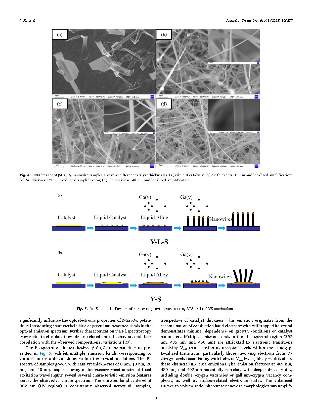
This investigation successfully demonstrated the controlled synthesis of β-Ga2O3 nanowires on SiC substrates via Au-catalyzed LPCVD. Through comprehensive characterization utilizing SEM, EDS, and PL spectroscopy, the critical influence of catalyst thickness on the morphological, dimensional, and structural properties of β-Ga2O3 nanowires was systematically elucidated. In the absence of Au catalyst, the samples exhibited no nanowire formation, underscoring the essential role of the catalyst in facilitating one-dimensional growth. With a 10 nm Au film, sparse nanowires with diameters of approximately 50 nm were successfully synthesized. Increasing the catalyst thickness to 20 nm resulted in a heterogeneous morphology comprising nanowires and a limited population of nanobelts with diameters of approximately 100 nm. Further increasing the Au film thickness to 40 nm produced densely packed nanowires, nanocolumns, and stacked nanobelts with diameters of approximately 150 nm, growing at an inclination relative to the substrate’s normal axis. The experimental results demonstrate that as the Au film thickness increases, the growth mechanism undergoes a transition from a predominantly VLS process to a hybrid VLS-VS regime, resulting in the concurrent formation of nanobelts and nanocolumns alongside nanowires. For the synthesis of well-defined, uniform β-Ga2O3 nanowire structures, the optimal condition was determined to involve the deposition of a 10 nm Au nanofilm. Under elevated temperature conditions, thermal decomposition of this Au film generated catalytic droplets with diameters of approximately 30 nm, which subsequently templated the growth of nanowires with diameters of approximately 50 nm. These findings establish a fundamental correlation between catalyst dimensions and resultant nanowire morphology, providing essential insights for the rational design and controlled synthesis of β-Ga2O3 nanowires with tailored properties for advanced optoelectronic applications.
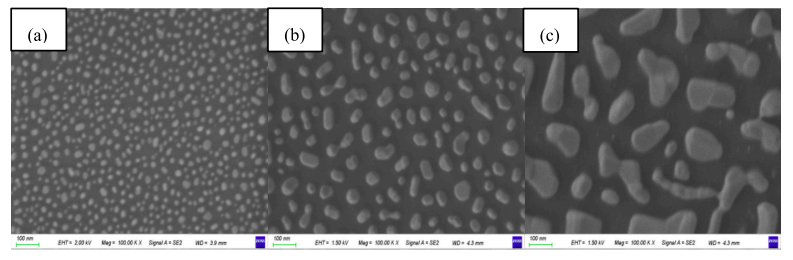
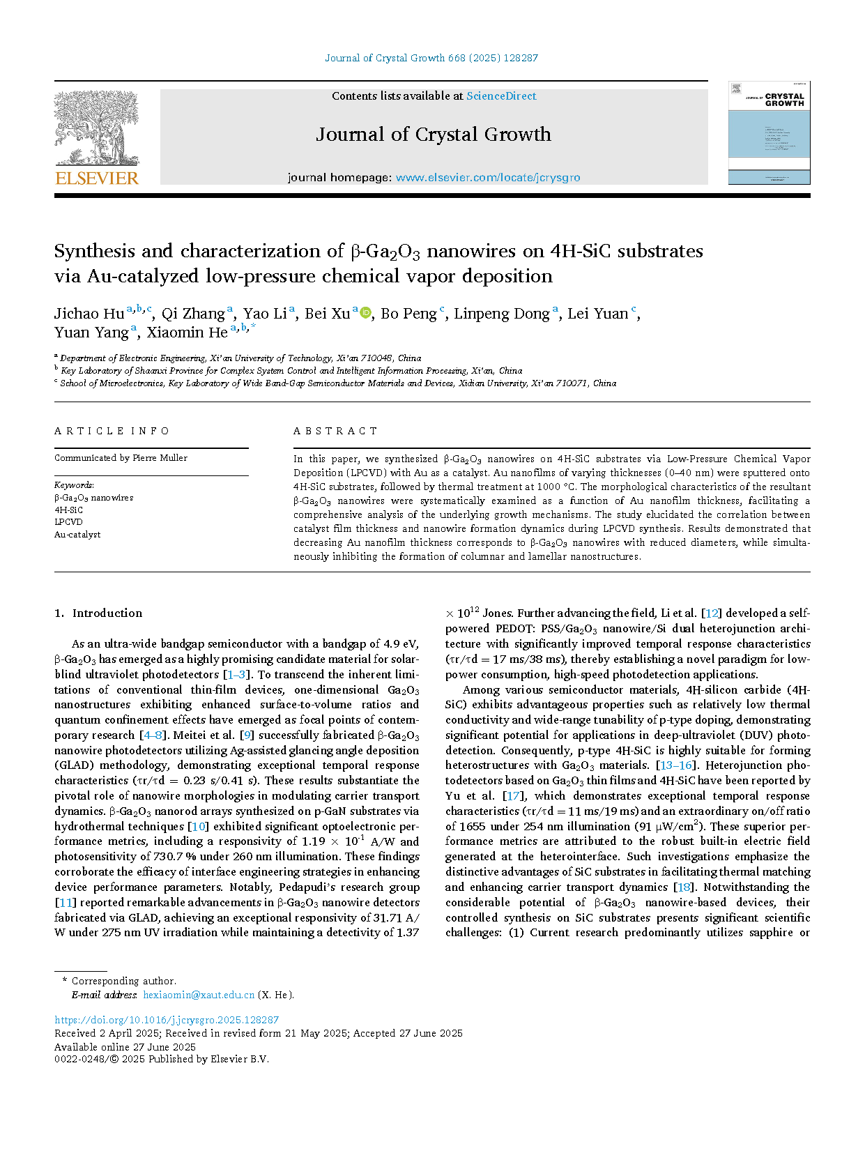
Fig. 1. SEM images of substrates annealed with different catalyst thicknesses: (a) Au thickness: 10 nm, (b) Au thickness: 20 nm, (c) Au thickness: 40 nm.
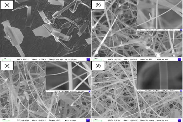
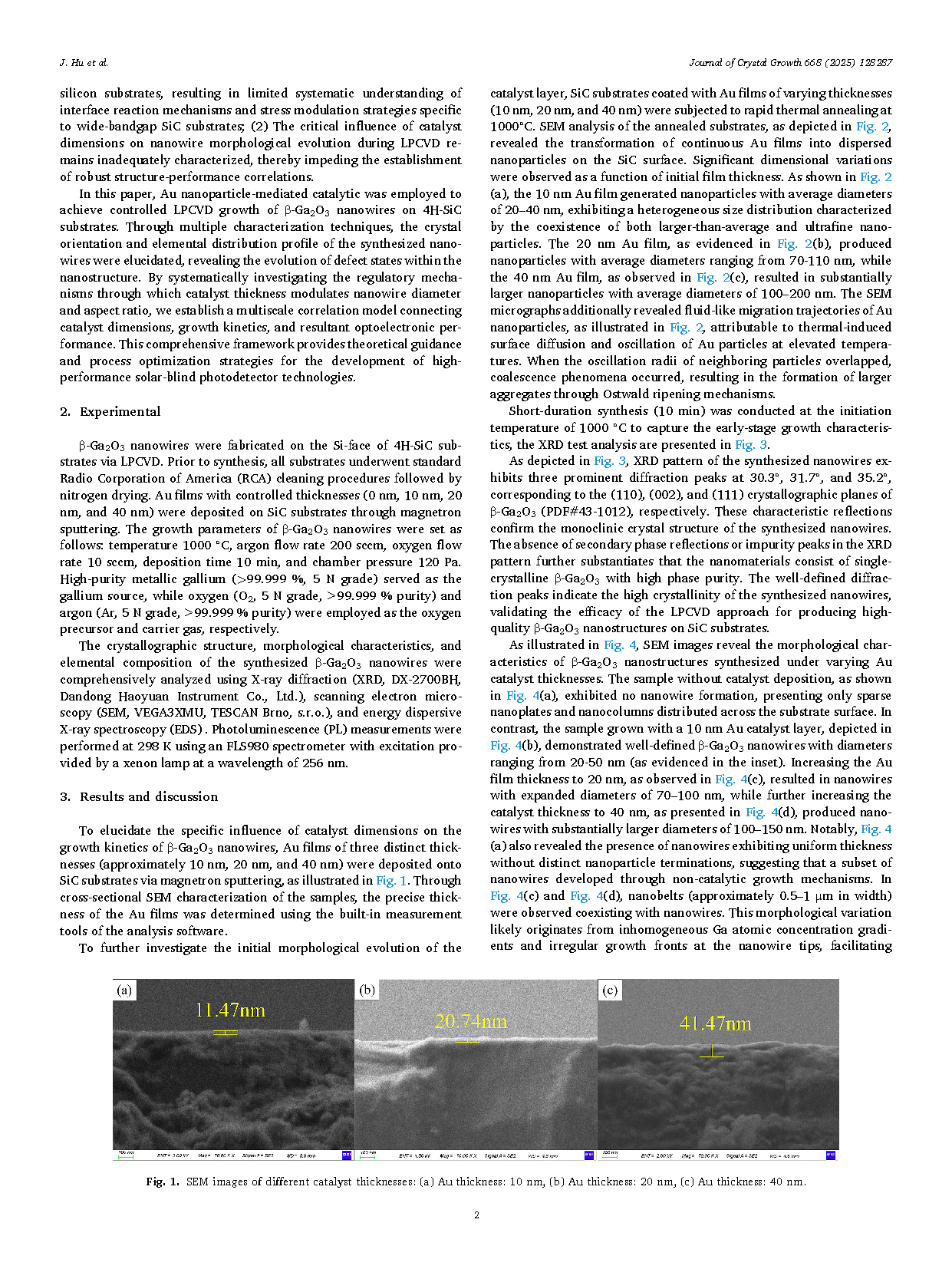
Fig. 2. SEM images of β-Ga2O3 nanowire samples grown at different catalyst thicknesses: (a) without catalysis; (b) Au thickness: 10 nm and localized amplification; (c) Au thickness: 20 nm and local amplification; (d) Au thickness: 40 nm and localized amplification.
DOI:
doi.org/10.1016/j.jcrysgro.2025.128287