


Paper Sharing
【Epitaxy Papers】Atomic interface structure and electronic properties at nanoscale rotated crystal in Ga₂O₃ homoepitaxial film
日期:2025-07-11阅读:659
Researchers from the Chungnam National University have published a dissertation titled "Atomic interface structure and electronic properties at nanoscale rotated crystal in Ga2O3 homoepitaxial film" in Applied Surface Science.
Abstract
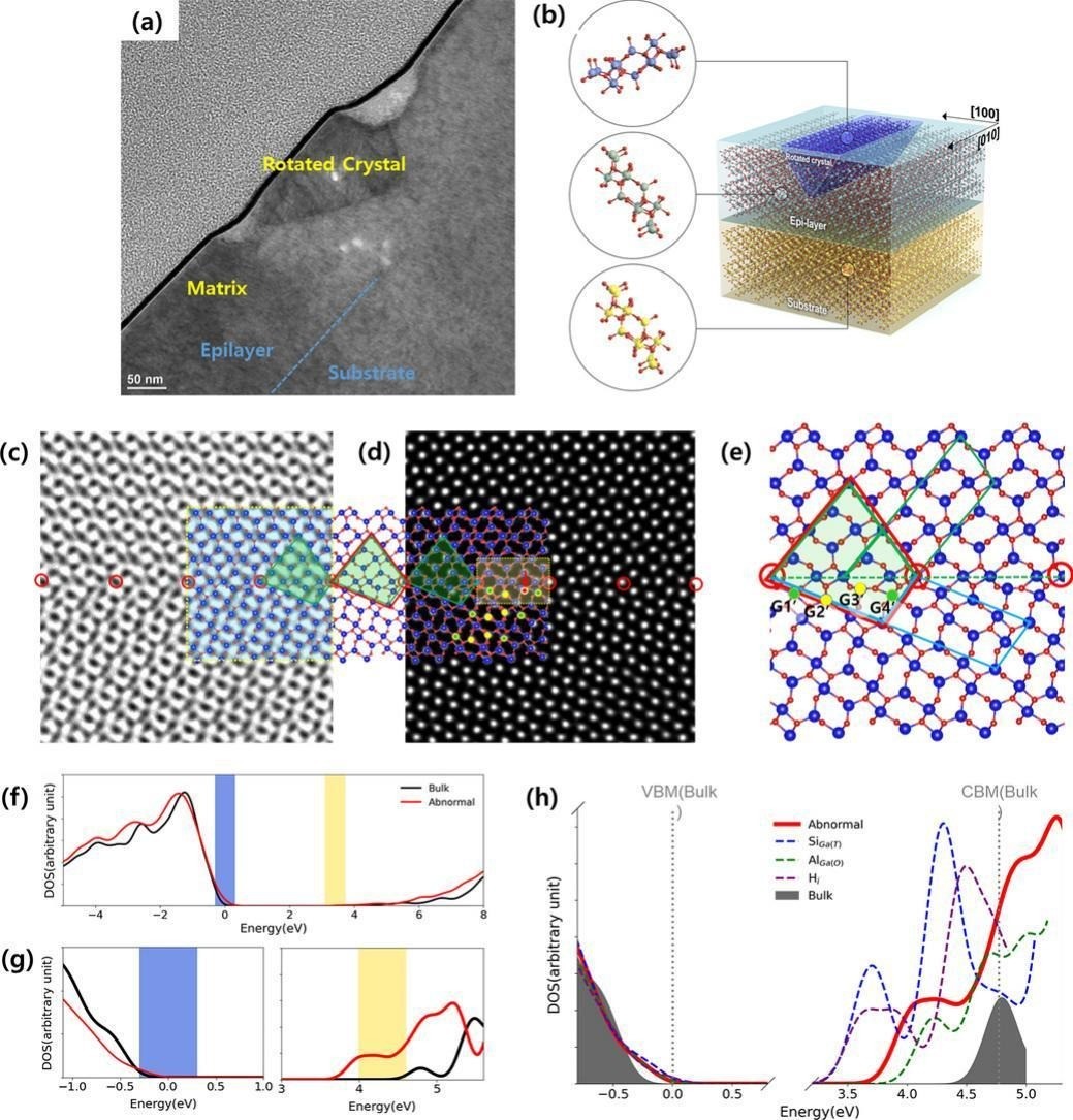
Although β-Ga2O3 is emerging as a next-generation power-electronics material, the understanding of two-dimensional defects is still lacking due to its complex crystal structure. We report a nanoscale rotated crystal of the β-Ga2O3 homoepitaxial layer and identify its crystal structure and electronic properties. By coordinating scanning transmission electron microscopy and density functional theory calculations, we analyze the rotated crystal in the homoepitaxial film with a crystallographic orientation of (-201)rotated//(202)matrix and [010]rotated//[010]matrix. The mismatch at the (-201)//(202) interface was as small as 0.0013, which is very close to zero. Sub-nanometer scale displacement of specific Ga atoms by ∼ 1.03 Å, appearing repeatedly and regularly at the interface was found. From DFT calculation the interface formation energy was determined to be 75.3 mJ/m2, which is very small compared to stacking fault energy of semiconductor materials. In addition, this defect itself induces delocalized deep-level states and we further calculated changes in band structure by impurity segregation at the boundary, which are difficult to passivate with segregation of impurities. These results provide a fundamental understanding into the atomic-scale interfacial structure at the locally formed nanoscale defect and their electronic property.
DOI:
https://doi.org/10.1016/j.apsusc.2025.163471
