Paper Sharing
【International Papers】Charge recovery by vacuum annealing in β-Ga₂O₃ multi-fin trench Schottky barrier diodes
日期:2025-07-11阅读:652
Researchers from the The Ohio State University have published a dissertation titled "Charge recovery by vacuum annealing in β-Ga2O3 multi-fin trench Schottky barrier diodes" in APL Electronic Devices.
Background
β-Ga2O3 is an ultra-wide bandgap semiconductor with a bandgap of 4.8 eV and a theoretical breakdown field strength of 8 MV/cm. This gives Ga2O3 a high Baliga Figure of Merit (BFOM) compared to Si, SiC, and GaN, making it attractive for high-power electronics. The availability of melt-grown bulk substrates makes β-Ga2O3 technology highly scalable and reliable and creates a competitive advantage over SiC and GaN. At this stage, the challenge with β-Ga2O3 is the absence of efficient P-type doping. Therefore, realizing devices closer to the theoretical limit is difficult if conventional planar vertical device architectures are used. In this context, the trench architecture is quite useful as it provides engineering flexibility and design scope to enable devices closer to the theoretical limit. Due to this reason, trench Schottky barrier diodes (SBDs) have been extensively explored due to their increased ability to sustain high electric fields. However, this also creates another difficulty: trench SBDs are conventionally fabricated using Inductively Coupled Plasma Reactive Ion Etching (ICP-RIE), which generally utilizes a Cl-based chemistry and results in charge compensation within the etched structure. We observed the effects of this charge compensation and resulting increase in on-resistance in our previous work. In addition, we found that the (010) plane is particularly susceptible to BCl3/Cl2-based dry-etch damage as compared to the (100) plane.
Abstract
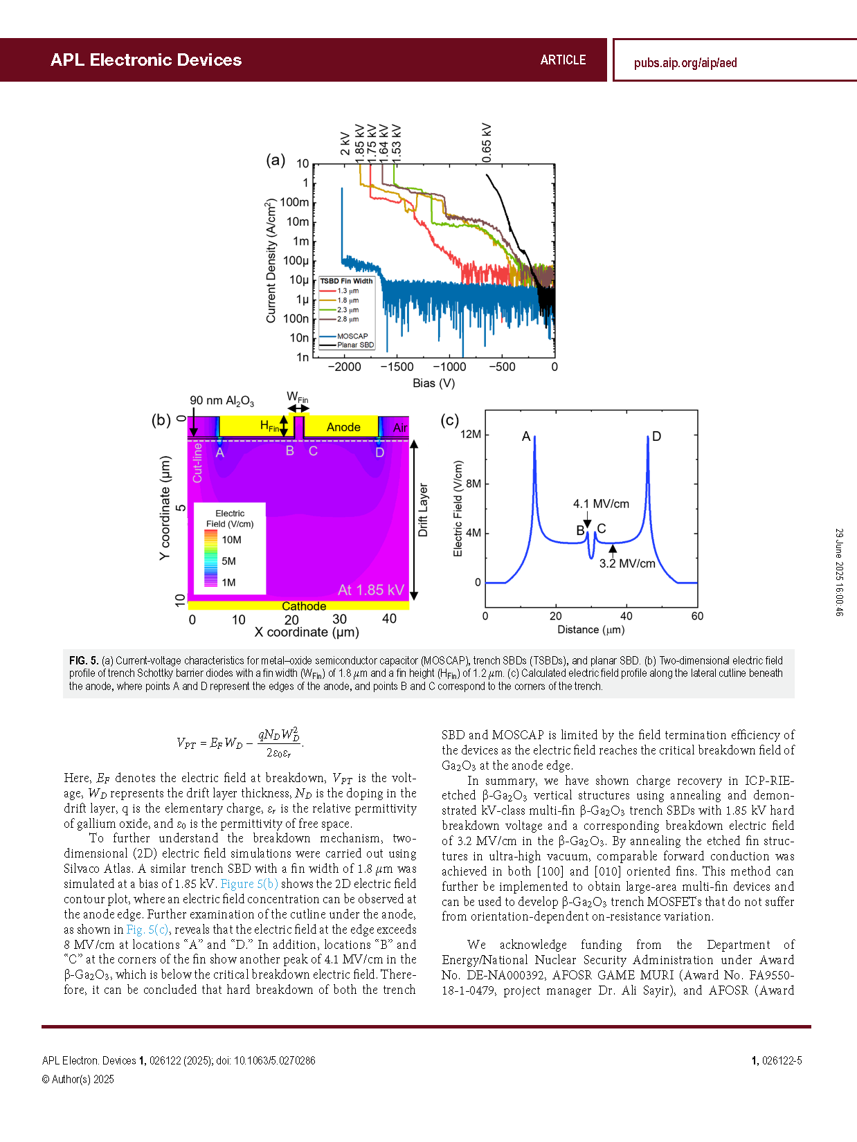
In this work, we have demonstrated charge recovery in (001) β-Ga2O3 vertical structures after reactive ion etching. The charge recovery is achieved by annealing the etched structures under ultra-high vacuum. Using the same technique, we have further demonstrated multi-fin trench Schottky barrier diodes oriented along [100] and [010] directions with comparable on-resistance. The trench Schottky barrier diodes showed a breakdown voltage as high as 1.85 kV with a punch-through breakdown electric field over 3.2 MV/cm.
Summary
In summary, we have shown charge recovery in ICP-RIE-etched β-Ga2O3 vertical structures using annealing and demonstrated kV-class multi-fin β-Ga2O3 trench SBDs with 1.85 kV hard breakdown voltage and a corresponding breakdown electric field of 3.2 MV/cm in the β-Ga2O3. By annealing the etched fin structures in ultra-high vacuum, comparable forward conduction was achieved in both [100] and [010] oriented fins. This method can further be implemented to obtain large-area multi-fin devices and can be used to develop β-Ga2O3 trench MOSFETs that do not suffer from orientation-dependent on-resistance variation.
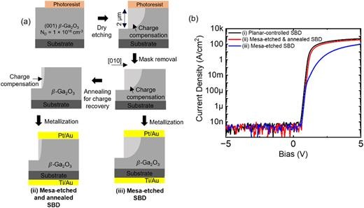
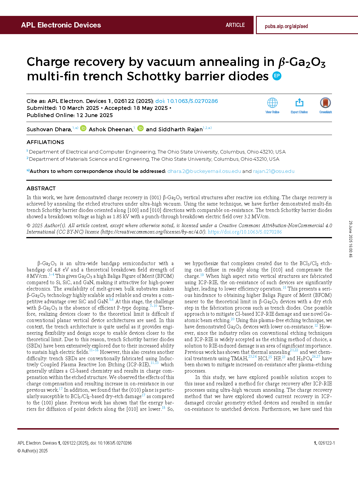
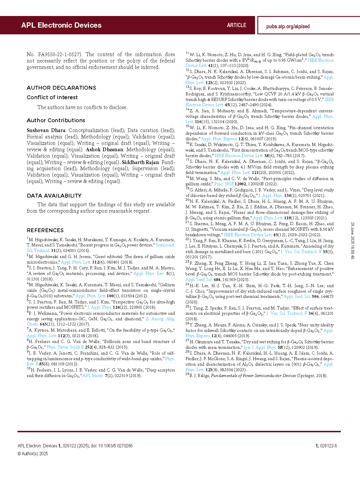
FIG. 1. (a) Schematic of device fabrication flow of mesa-etched SBDs for charge recovery experiment. (b) Comparison of current–voltage (J–V) profile for planar controlled SBD, mesa-etched SBD, and mesa-etched and annealed SBD.
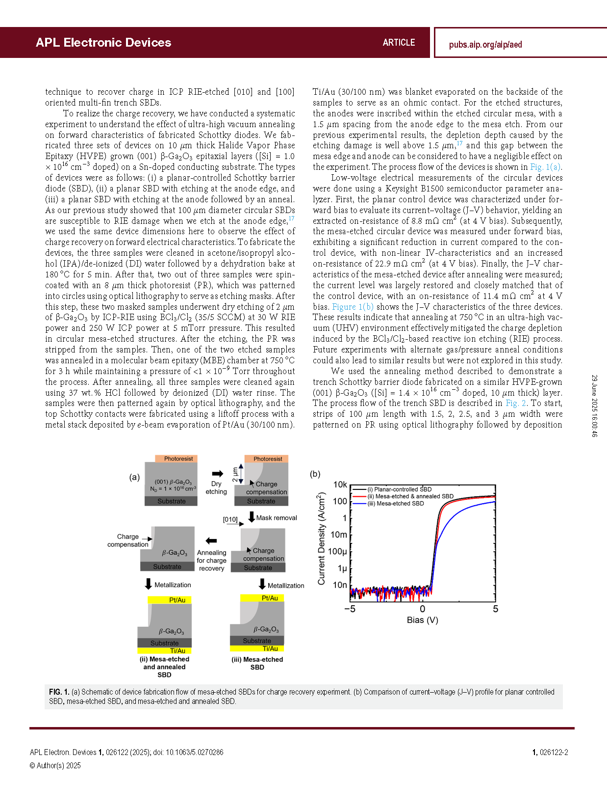
FIG. 2. Process flow of multi-fin trench SBD using RIE and ultra-high vacuum annealing.
DOI:
doi.org/10.1063/5.0270286