Paper Sharing
【Domestic Papers】Switching Reliability of NiO/Ga₂O₃ Bipolar Junction Evaluated by a Circuit Method
日期:2025-07-14阅读:663
Researchers from The University of Hong Kong have published a dissertation titled "Switching Reliability of NiO/Ga2O3 Bipolar Junction Evaluated by a Circuit Method" in ISPSD 2025.
Background
Ultra-wide bandgap (UWBG) semiconductor Ga2O3 has garnered significant research attention due to its potential applications in power electronics, which are critical for advancing carbon neutrality goals. Ga2O3 stands out as a particularly promising candidate owing to its ultra-wide bandgap, high critical electric field, controllable n-type doping, and the availability of large-area wafers. However, the effective p-type doping remains unfeasible in Ga2O3. As an alternative, the heterojunction formed by n-type Ga2O3 and p-type NiO has been widely recognized as one of the most successful building blocks for Ga2O3 devices, enabling high-voltage devices up to 10 kV, as well as the avalanche and surge-current robustness.
Abstract
Ultra-wide bandgap (UWBG) NiO/Ga2O3 bipolar junction has emerged as a critical building block for diverse Ga2O3 power devices, owing to the high breakdown field and avalanche capability. However, the reliability of this bipolar UWBG junction under dynamic switching conditions remains unexplored. In this work, we for the first time characterize the circuit-level switching reliability of large-area NiO/Ga2O3 diodes during continuous 10A/650V and 10A/1.2kV inductive switching. The parametric shift is extracted by reconstructing a large-signal, dynamic I-V curve using the voltage and current waveforms recorded in each switching cycle. The junction shows a decrease in both turn-on voltage (VON) and differential on-resistance (RON-D) by up to 0.25 V and 36%, respectively, after 107 switching cycles. Such shifts are found to be mitigated under higher switching voltage. Moreover, the circuit test data are compared to the parametric shifts under DC stress. While the parametric shifts under both tests can be characterized by a trapping/de-trapping time constant of ~4200 s, the magnitude of parametric shifts are higher under the switching stress. The underlying physical mechanisms are discussed. These results provide key references to converter application of NiO/Ga2O3- based power devices and suggest the importance of switching-based methodology for device reliability evaluation.
Conclusion
In summary, this work presents the first reliability study of NiO/Ga2O3 UWBG devices under application-like switching stresses involving the alternating forward current and reverse bias. This switching reliability test is performed by a circuit test, relying on the large-signal dynamic I-V reconstructed using the current and voltage waveforms. Our study reveals a decrease in VON and RON-D to be the major parametric shift of NiO/Ga2O3 junction under practical switching conditions. Such shifts are fully recoverable and governed by deep-level trapping/de-trapping with a time constant of 4200 s. The parametric shifts under this circuit test are found to be higher than those in the DC test, suggesting the significance of a circuit-based switching methodology. These results key reference for the circuit application of NiO/Ga2O3-based UWBG devices.
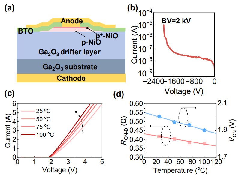
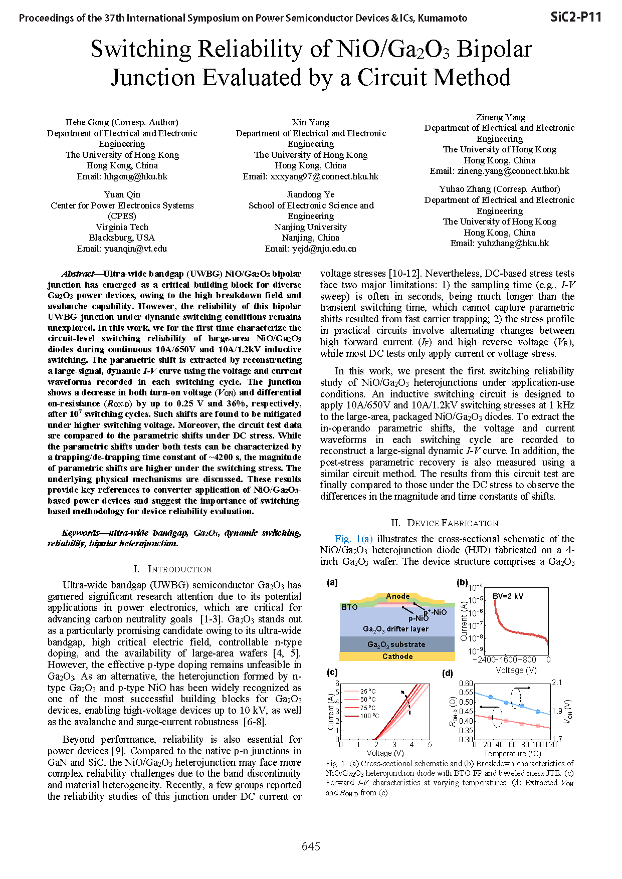
Fig. 1. (a) Cross-sectional schematic and (b) Breakdown characteristics of NiO/Ga2O3 heterojunction diode with BTO FP and beveled mesa JTE. (c) Forward I-V characteristics at varying temperatures. (d) Extracted VON and RON-D from (c).
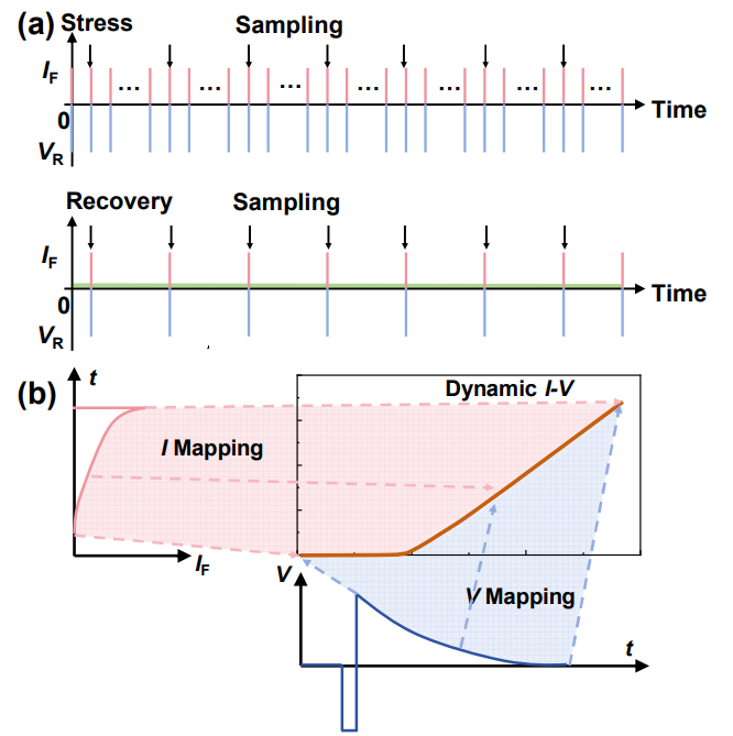
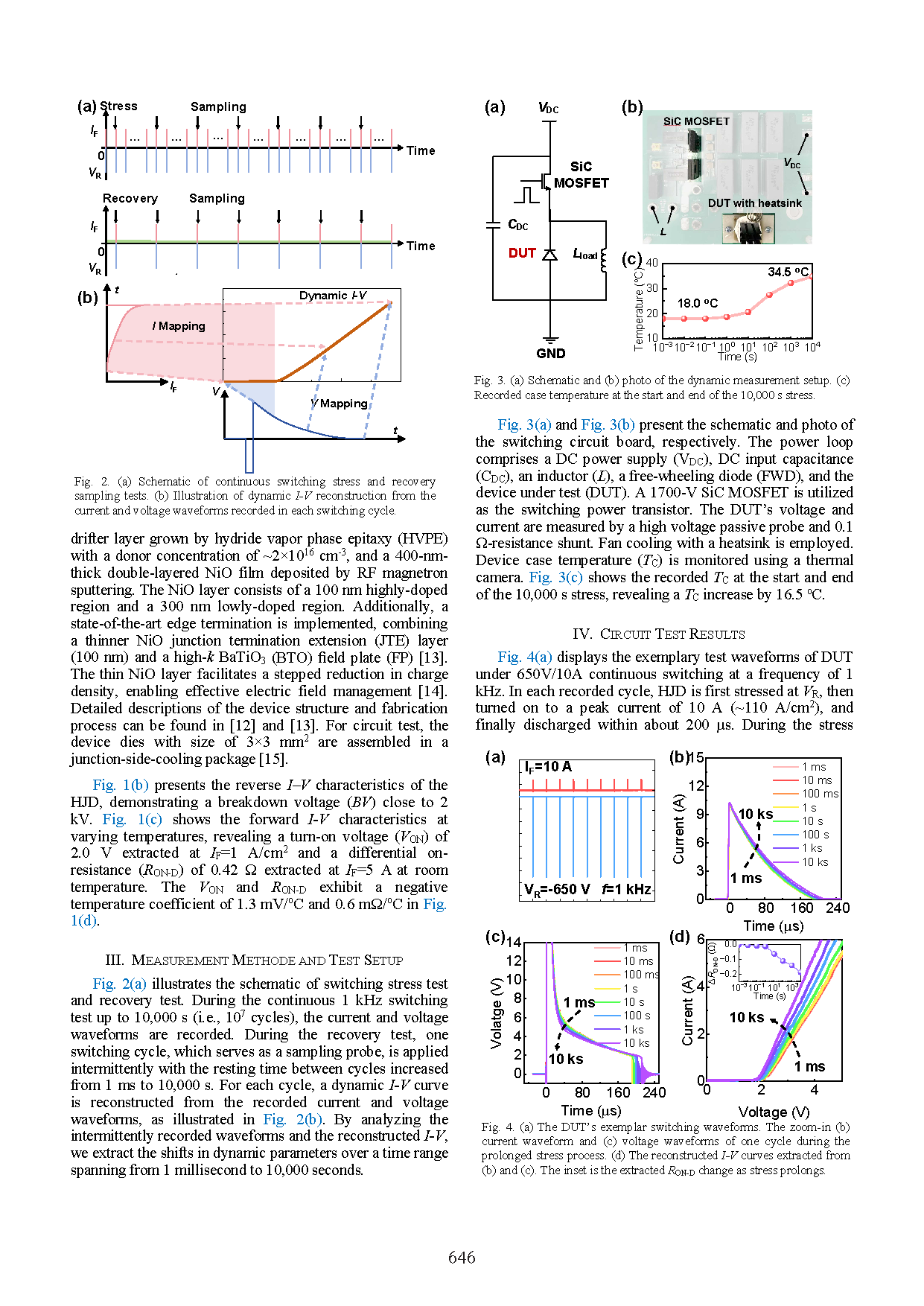
Fig. 2. (a) Schematic of continuous switching stress and recovery sampling tests. (b) Illustration of dynamic I-V reconstruction from the current and voltage waveforms recorded in each switching cycle.