Paper Sharing
【Member Papers】High-Performance Cu₂O/Ga₂O₃ Heterojunction Diodes for Power Electronics
日期:2025-07-14阅读:696
Researchers from the Southern University of Science and Technology and Shenzhen Polytechnic University have published a dissertation titled "High-Performance Cu2O/Ga2O3 Heterojunction Diodes for Power Electronics" in EDTM 2025.
Project Support
This work was supported by National Natural Science Foundation of China (Grant No: 62274082). Research on mechanism of source/drain ohmic contact and the related GaN p-FET (Grant No: 2023A1515030034). Research on high-reliable GaN power device and the related industrial power system (Grant No: KZQB-KCZYZ-2021052). Study on the reliability of GaN power devices (Grant No: JCYJ20220818100605012). Research on novelty low-resistance Source/Drain ohmic contact for GaN p-FET (Grant No: JCYJ20220530115411025). Research on the key technology of 1200 V SiC MOSFETs (Grant No: JSGG20220831094404008). “5G Frontier” project Micro-Nano processing platform (Grant No: K2023390010). High level of special funds (G03034K004). The authors also acknowledge the assistance of SUSTech Core Research Facilities.
Background
Gallium oxide (Ga2O3) has emerged as a promising candidate for applications in high-voltage power electronics, owing to its ultra-wide bandgap of 4.5-4.8 eV, high Baliga’s figure-of-merit, and high critical breakdown field (8 MV/cm) superior to Si, SiC, and GaN materials. Additionally, the availability of melt-grown single crystal Ga2O3 substrates enhances their potential for cost-effective and high-quality homoepitaxy. However, the lack of p-type doping capability still displays a critical limitation for Ga2O3 bipolar power electronics. To address this challenge, the integrating n-type Ga2O3 with p-type semiconductors presents an effective strategy for fabricating p-n heterojunction diodes (HJDs), thereby paving the way for high-voltage power electronics applications.
Abstract
In this work, high-performance Cu2O/Ga2O3 heterojunction diodes (HJDs) are demonstrated via the construction of a double-layer of Cu2O with graded hole concentrations. Taking advantages of the single-layer HJDs featuring p+ Cu2O layer and p- Cu2O layer, respectively, the double-layer HJD achieves a high breakdown voltage of 2430 V, further yielding a power figure-of-merit of 0.91 GW/cm2. This offers a promising pathway for advancing the application of Ga2O3-based HJDs in future power electronics.
Conclusion
This study presents an optimization strategy for the Cu2O/Ga2O3 HJDs by adjusting the hole concentration in Cu2O layers. The fabricated DL HJD exhibits a remarkable BV of 2430 V, a Ron,sp of 6.52 mΩ·cm2, and a VON of 1.8 V. Furthermore, it yields a high PFOM of 0.91 GW/cm2. This work provides a practical and effective approach to enhancing the performance of Cu2O/Ga2O3 HJDs.
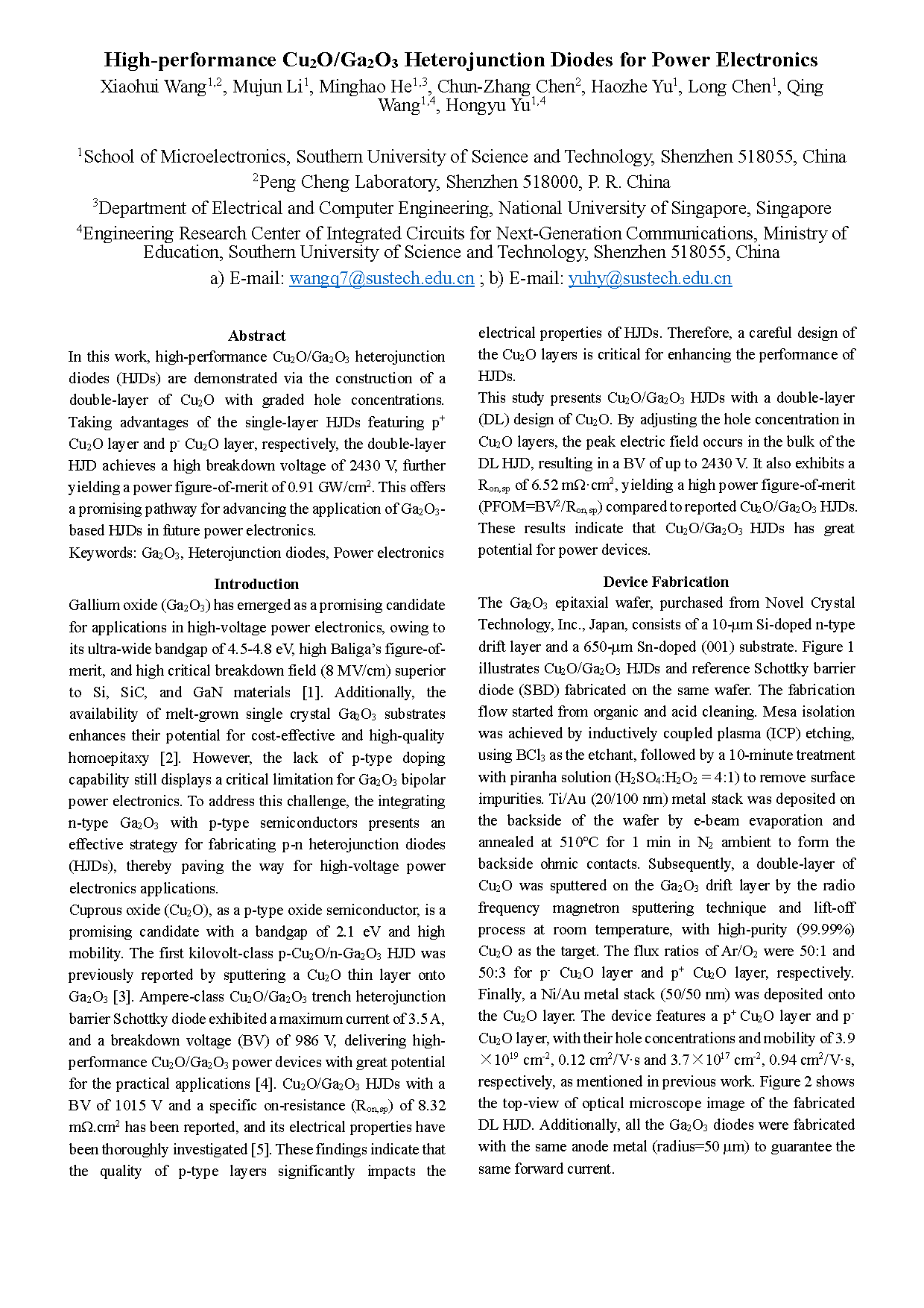
Fig. 1. Cross-section schematic of Cu2O/Ga2O3 HJDs with various devices structures and their fabrication flow.

Fig. 2. Top-view of optical microscope image of the fabricated DL HJD.
DOI:
doi.org/10.1109/EDTM61175.2025.11041080