Paper Sharing
【Member Papers】Recent Advances in Device-Level Thermal Management Technologies for Wide Bandgap Semiconductor: A Review
日期:2025-07-15阅读:998
Researchers from the Xidian University have published a dissertation titled "Recent Advances in Device-Level Thermal Management Technologies for Wide Bandgap Semiconductor: A Review" in IEEE Transactions on Electron Devices.
Project Support
This work was supported in part by the National Natural Science Foundation of China under Grant 62304170 and Grant 62374122, in part by Guangdong Basic and Applied Basic Research Foundation under Grant 2023B1515040024 and Grant 2022A1515111137, in part by the Xidian University Specially Funded Project for Interdisciplinary Exploration under Grant TZJH2024057, and in part by the National Key Research and Development Program of China under Grant 2021YFB3601900.
Background
WIDE bandgap (WBG) semiconductors have been widely used in power and radio frequency (RF) electronics because of their superior figures of merit (FoMs), particularly in the field of electrical grids, high-speed transportation, and industrial electronics. In the past year of 2023, the global market for GaN power devices, one of the most typical WBG semiconductors, has reached U.S. $17.5 billion and the predicted annual growth rate is expected to be 22.5%. In particular, an increasing number of commercial GaN products have been released with higher FoMs, higher energy conversion efficiencies, and higher frequencies for power switching application. For example, the industry’s first CMOS driver-GaN power switch technology based on 300-mm GaN-on-Si was reported by Intel Corporation using a monolithic integration process in 2023 IEDM. Fujitsu Ltd. reported a high-power RF GaN HEMT that presented a high drain current of 1470 mA/mm with a record output power density of 24.4 W/mm in the X-band and an operating voltage of 110 V in 2023. In 2024, a GaN on SiC HEMT with superior performance using the thermal chemical vapor deposition (CVD) process was reported by the same company, which achieves an output power density of 31.0 W/mm at the X-band and 90-V operating voltage. Obviously, the WBG and even ultra-WBG (UWBG) semiconductors will continue to develop rapidly with the global popularization of 5G communication, electric vehicles and other fields.
Abstract
Wide bandgap (WBG) and ultra-WBG (UWBG) semiconductor devices exhibit superior performance with higher breakdown voltage and lower on-resistance compared to Si-based devices, rendering them highly competitive in the field of electric energy conversion and communication. Especially, GaN, as one of the representative materials in WBG semiconductors, has progressed to the stage of industrial realization, and the new generation of UWBG semiconductors such as Ga2O3 has become a popular research focus in the last decade for power electronics applications. However, the primary challenge faced by these advanced semiconductor devices is thermal management, particularly in high-power application, which leads to a serious degradation in electrical performance and long-term reliability. Therefore, there is an urgent need for effective thermal management technologies. This review comprehensively summarizes recent advances in device-level thermal management techniques for WBG and UWBG semiconductors, ranging from internal device structure optimization to a series of external strategies for enhancing thermal diffusion. These strategies include enhancing the internal thermal dissipation through device architecture optimization, substrate thinning, high thermal conductivity substrate bonding and coverage, flip chip package, active method of microchannel cooling, and transient thermal management techniques. Finally, we discuss the existing technical challenges, potential solutions, and further development opportunities in thermal management techniques, with the aim of addressing the critical thermal dissipation issue to facilitate the further industrialization of WBG and UWBG semiconductors.
Outlook
Although the above-mentioned cooling methods are useful in the current thermal management strategy, new insight and technique are also in demand to promote the development of high-power devices. Here, we propose several potential research opportunities for thermal management as follows: 1). Current active cooling technologies primarily involve liquid cooling such as microchannel cooling, which face a series of issues including poor electrical isolation and leak risk. Therefore, a new type of solid-state active cooling technology is expected to provide solid guarantee for device stability. Electrocaloric materials present behavior of absorption or release of heat under the applied external voltage, which can be integrated on the device bottom or surface to form a “refrigeration air conditioner” at the chip level. Moreover, this technique is compatible with the standard device fabrication process by deposition strategy, showing the advantages such as simple process and low manufacturing cost. 2). A PN-junction type semiconductor can build a small thermoelectric refrigerating unit on chip backside based on Peltier effect, which could produce cooling effect for power chip. Through thermoelectric material deposition, photolithography, etching and metal deposition process, the micro thermoelectric refrigerating unit could be easily formed on chip backside. Certainly, these techniques still need to be further optimized to achieve maximized cooling effect.
In summary, to achieve excellent thermal dissipation and to accelerate the deep industrialization of WBG and UWBG semiconductors, the relevant power devices should be designed from a thermal perspective with an appropriate configuration, the integration of high thermal conductivity materials for wrapping, and substrate cooling engineering to comprehensively enhance thermal dissipation capabilities. It is expected that major progress in these aspects will substantially advance the rapid development of WBG and UWBG semiconductors for power electronics application.
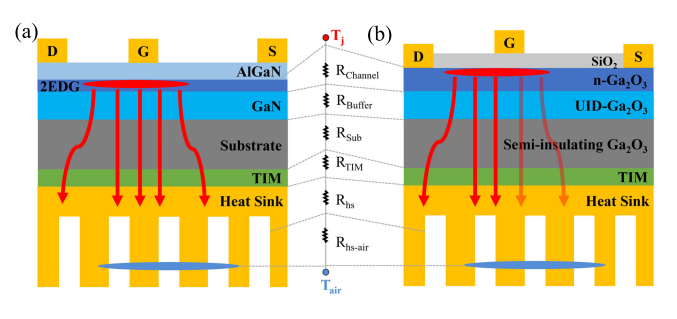
Fig. 1. Thermal dissipation pathway and equivalent thermal resistance model for (a) GaN HEMT and (b) Ga2O3 MOSFET.
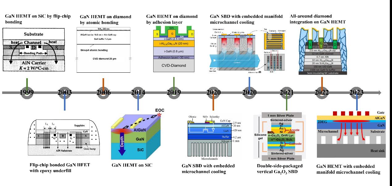
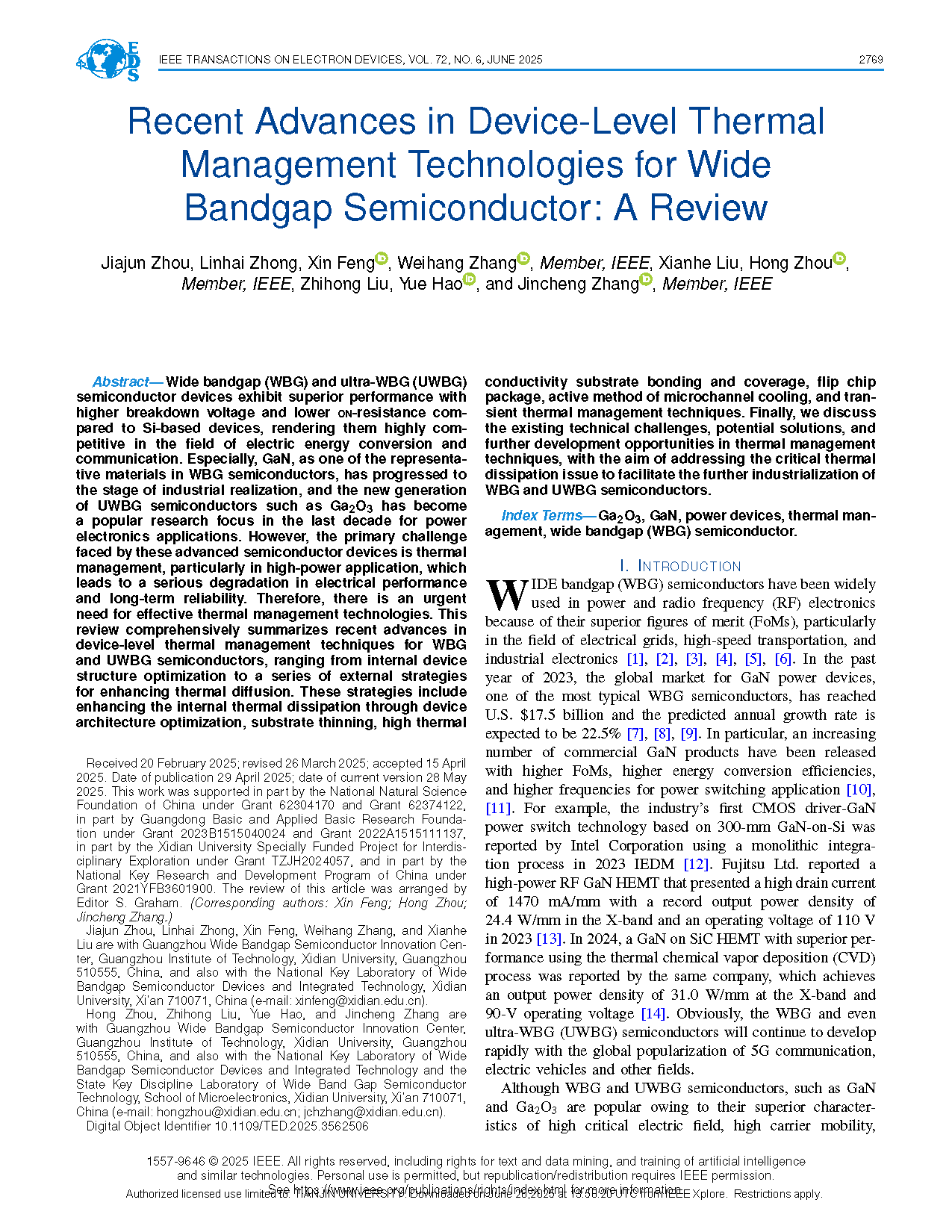
Fig. 2. Brief timeline of the development of advanced heat-management technologies for WBG/UWBG.
DOI:
doi.org/10.1109/TED.2025.3562506