


Discover
【Knowledge Discover】How does UCSB Gallium Oxide 20kV Photoconductive Auxiliary Switching Device PCAS Have Better Thermal Reliability and Overload Capability Than Traditional Devices?
日期:2025-07-20阅读:1384
(This article is reposted from a personal WeChat offical account.)
In the past few days, I went to a Gallium Oxide industry development technology event to study, and I felt that the popularity of the Gallium Oxide industry has surpassed the increasingly involuted Silicon Carbide.
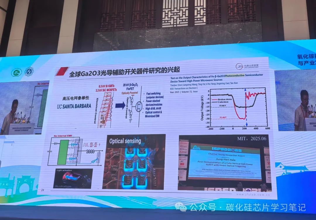
This Gallium Oxide industry technology event was very well organized, and I met a lot of teachers and seniors from industry and research institutions, as well as young researchers. I had an in-depth exchange with many friends about the possibility of Gallium Oxide PCAS devices, going up to 20kV, 30kV..., and learning about the integrated control of MIT wide bandgap semiconductor devices Tom's large group of 650V ordinary silicon-based optocouplers mature industrial technology.
Although we now have the reference of the technical plan from the United States, if we want to promote domestic resource support, especially the resource support of local and national projects, the comparison at the technical level needs to be discussed clearly.
I just had the honor to have an in-depth exchange with a young expert who has been deeply involved in the field of power grid robustness and ultra-high voltage for more than 20 years, and discussed three issues:
1. How to achieve 10,000 volts and 10,000 amps of Gallium Oxide PCAS in the United States? Why is it easier than Silicon Carbide?
2. How do GO PCAS devices in the United States dissipate heat? Isn't Gallium Oxide poor thermal conductivity?
3. Why can the US Gallium Oxide PCAS construct better overload reliability and high-voltage grid rosterity ?
Let's discuss them one by one
1.How to achieve 10,000 volts and 10,000 amps of Gallium Oxide PCAS in the United States? Why is it easier than Silicon Carbide?
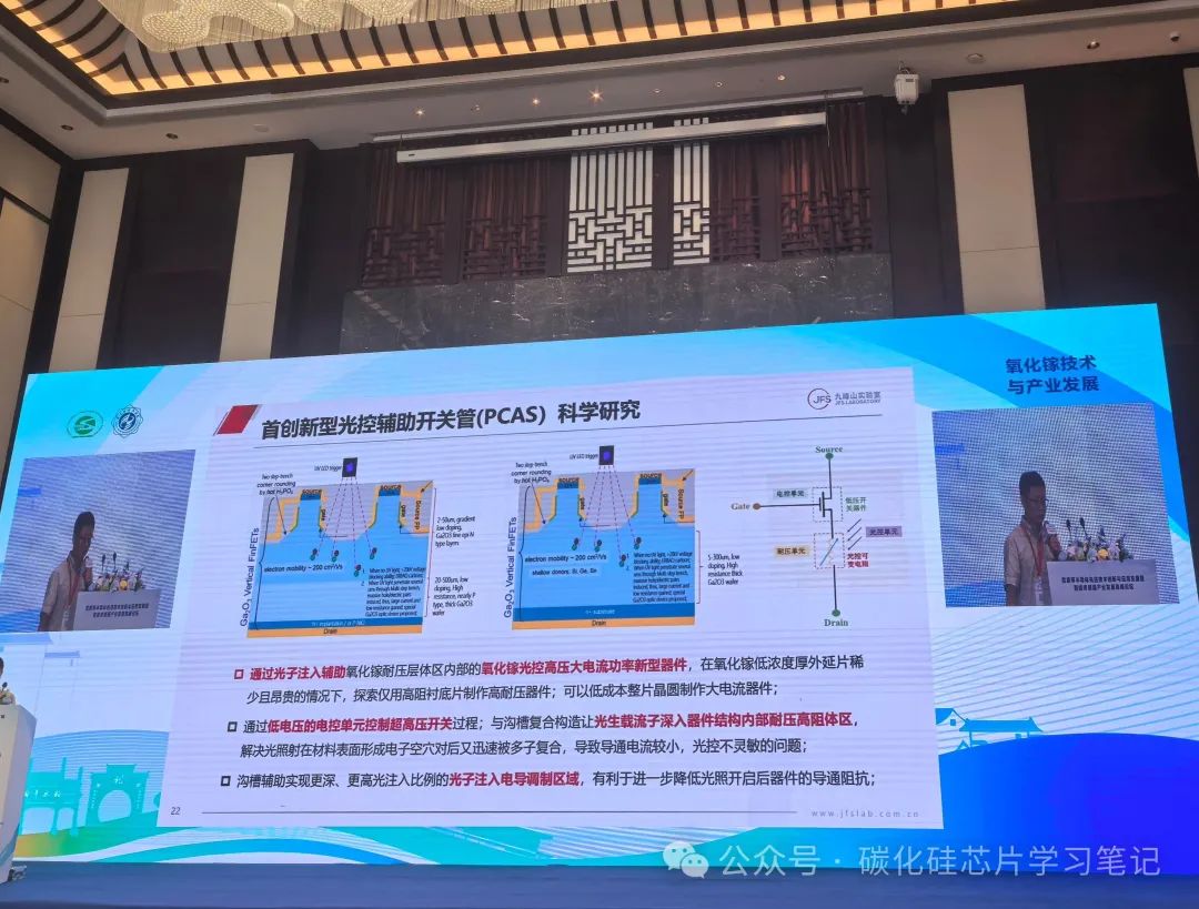
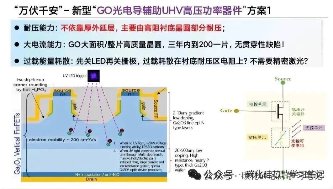
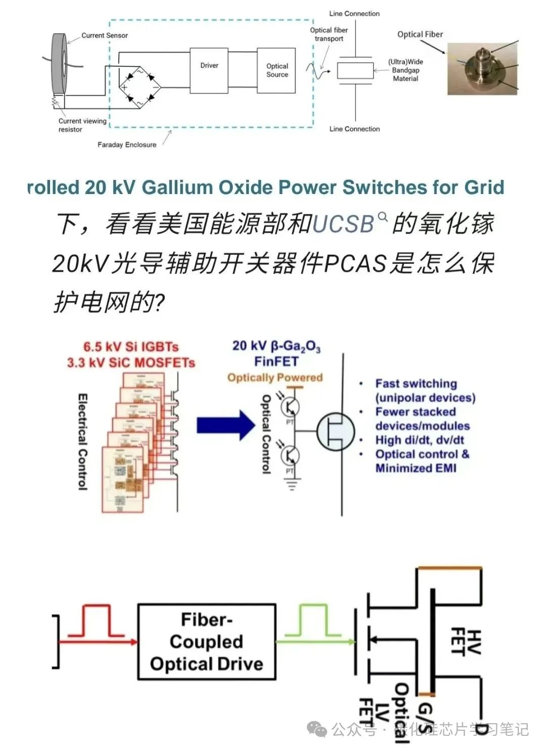
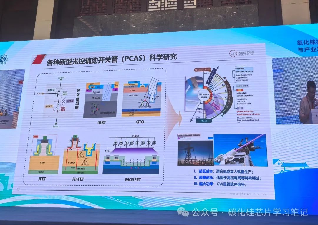
Gallium Oxide can achieve 10,000 volts and 1,000 amps more easily than silicon carbide In the past two months, the publication of the world's first and second articles on Gallium Oxide light guide switching devices has been published from the 20kV of the Lawrence Laboratory in the United States and the measured data of Gallium Oxide 30kV devices by our National University of Defense Technology teacher Wang Langning, which has proved this. Think about it, this is a breakthrough in technical indicators that hundreds of research teams around the world have not achieved in the past thirty or forty years!
After all, Gallium Oxide is an ultra-wide bandgap, which is much stronger than Silicon Carbide materials! The innate mission is to be able to withstand ultra-high pressure.
Not to mention current and cost. Gallium Oxide is a melt method long crystal, the defects of the monoclinic crystal system long crystal are easy to close, and there is no penetrating defect after maturity, the future eight-inch wafer is 200 yuan a piece, learn the high-voltage silicon pile technology of the past 60 years, our two-inch wafer area to make a whole device, easily tens of thousands of volts and 1000 amps.
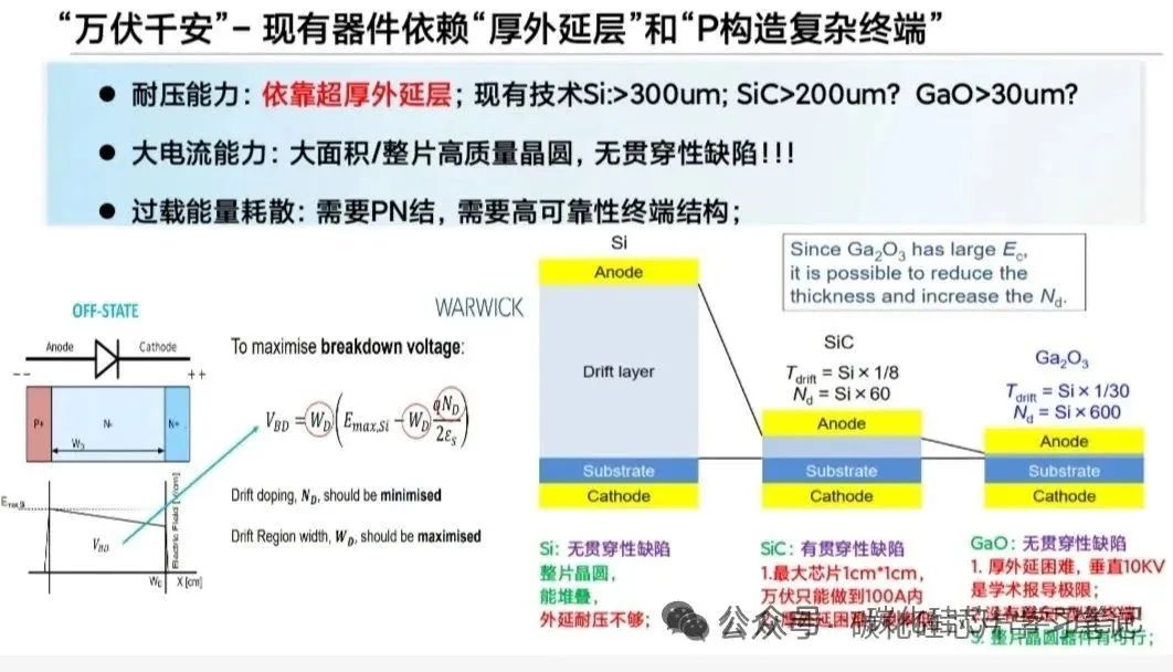
Silicon Carbide has been made for thirty or forty years, but it has not been able to achieve 10,000 volts and 1,000 amps. Even today, Silicon Carbide 1200V devices with an area of more than 1cm*1cm have almost no yield, let alone ultra-high voltage.
An early joke used to be that one test method to measure the defect detection of Silicon Carbide wafer microtubules was to sprinkle some water on the wafer and pressurize it to see if there was any leakage and how fast the leakage rate was. It is said that this is really not a joke, it was really tested like this for a while. 4H Silicon Carbide is a hexagonal columnar crystal system, which is inherently prone to penetrating defects. If you can find a crystal system that is tilted left and right like Gallium Oxide, the defect is easy to close.
2.How do GO PCAS devices in the United States dissipate heat? Isn't Gallium Oxide poor thermal conductivity?
The second is the heat dissipation of Gallium Oxide PCAS. Let's first take a look at why traditional switching devices have thermal reliability problems.
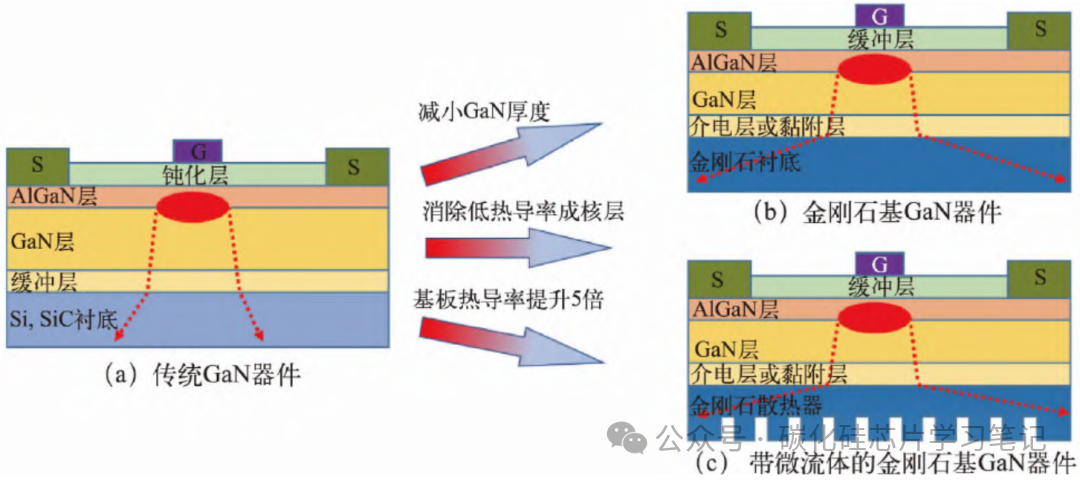
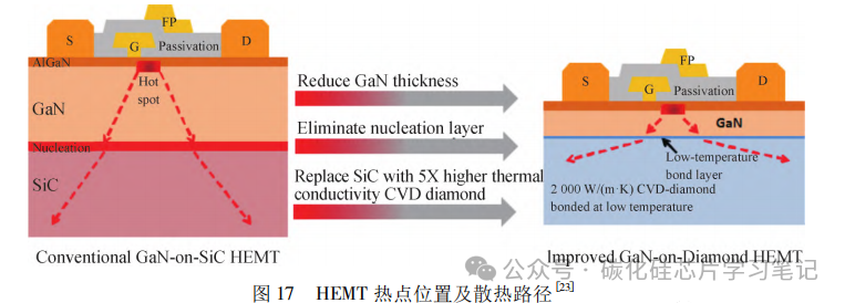
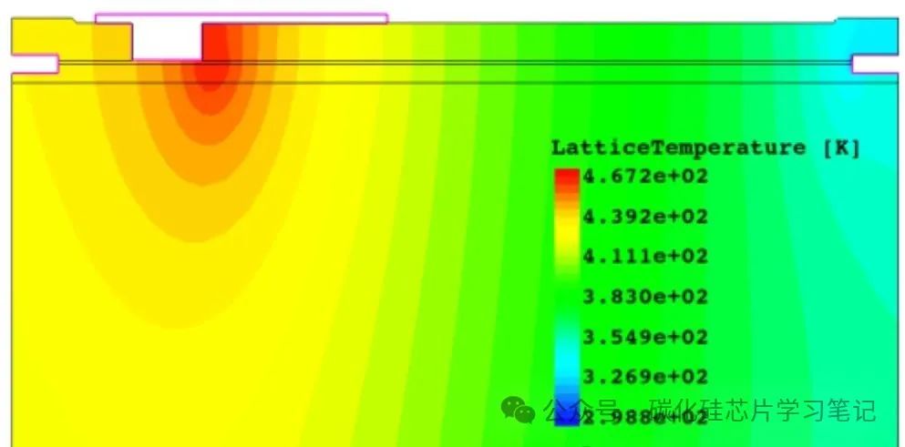
The core is that the on-resistance and heat generation of the existing traditional switching devices are mainly a few micron-sized hot spots in the channel area, as well as a few dozen um in the upper part of the epitaxial drift layer, so GaN HEMT is always thermal breakdown near the bottom of the grid, while Silicon Carbide short-circuit resistance is resistant to SCWT always burning the gate and source metal near the channel area to melt and slag. In addition, the diamond heat dissipation cannot withstand too much, and the instantaneous heat is concentrated in a few microns or more than a dozen microns.
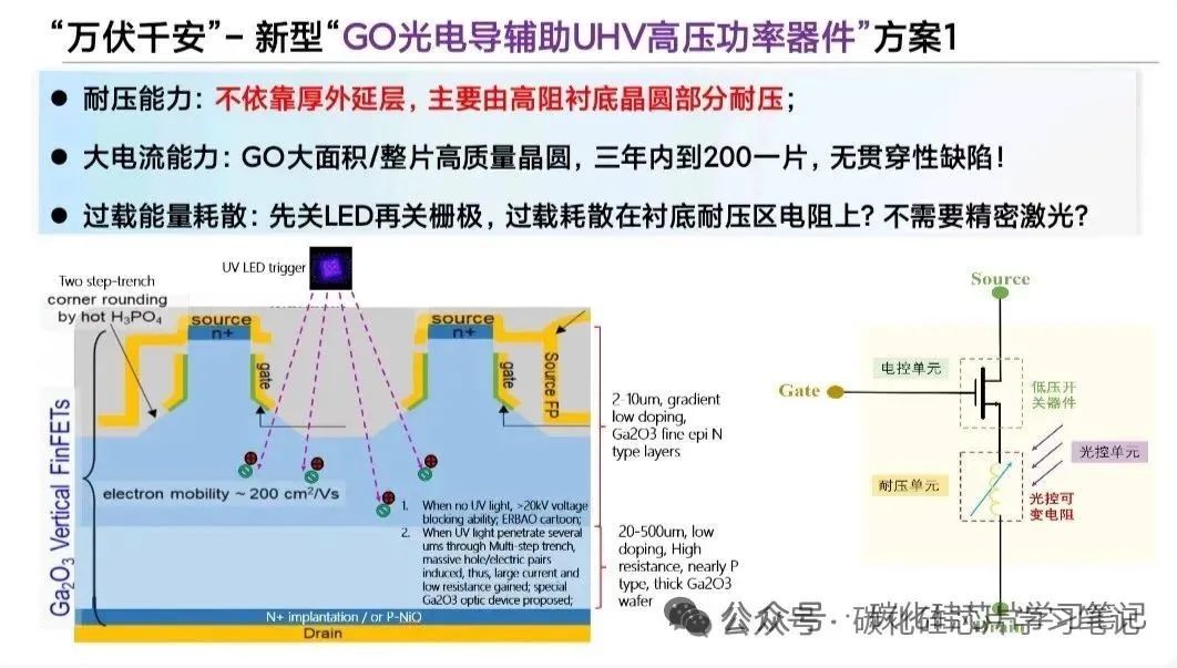
This is not the case with Gallium Oxide PCAS photoguide auxiliary switching devices. Its withstand voltage, conduction, and overload energy dissipation are widely distributed throughout the wafer substrate region rather than the device's low-voltage switching zone.
3.Why can the US Gallium Oxide PCAS construct better overload reliability and high-voltage grid rosterity ?
Unlike traditional silicon or Silicon Carbide IGCT/IGBT/GTO and other switching devices, in the new Gallium Oxide PCAS photoconductive auxiliary switching device technology developed at the end of 2024, the heat of switching and overload energy is dispersed in the entire wafer with an area of several hundred square centimeters, and the substrate wafer area of a few hundred microns or even a few millimeters, then the heat dissipation and heat resistance reliability is not a problem. Not a problem at all!
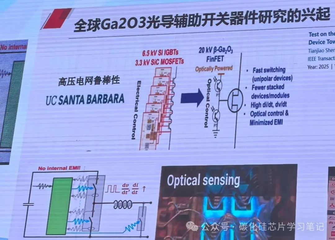
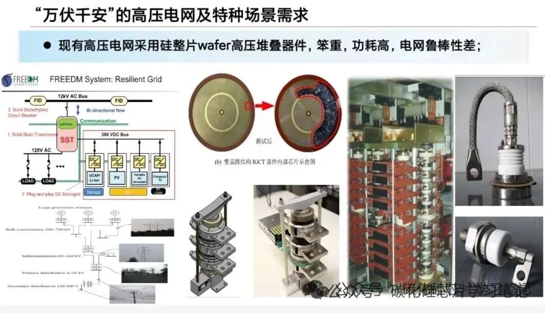
Therefore, it makes sense that the United States says that Gallium Oxide PCAS devices are used to strengthen the robustness of high-voltage power grids!
In addition, the high-voltage power grid needs full control devices, the traditional optical guide switch PCSS is not fully controlled, and it is easy to have large photocarrier secondary composite luminescence false triggering and rear pulse, but the new Gallium Oxide PCAS light guide auxiliary switch device can be fully controlled. The overload is all over the entire wafer substrate, which is definitely better than traditional switching devices.
