


News Trends
【Domestic News】Jiachuang Future Semiconductor Achieved Global Leadership in Core Indicators of Gallium Oxide Epitaxy for Silicon Carbide Substrates
日期:2025-07-25阅读:1045
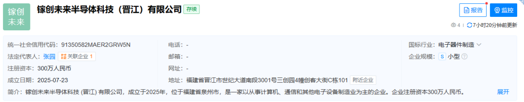
Recently, Jiachuang Future Semiconductor Technology (Jinjiang) Co., Ltd. was officially established in Jinjiang City, Fujian Province, dedicated to the research and development and industrialization of Gallium Oxide (β-Ga₂O₃) heteroepitaxial materials. The founding team is composed of a group of doctoral students from Xidian University. The core members all have over ten years of experience in the research or industry of Gallium Oxide/Silicon Carbide materials. Their technology is based on the State Key Discipline Laboratory of Wide Bandgap Semiconductor Technology and the National Engineering Research Center for Wide Band Gap Semiconductors of Xidian University. At present, more than 20 related patents have been applied for in areas such as Gallium Oxide epitaxial growth, defect control, doping simulation and process, and over 30 SCI papers have been published.
Gallium Oxide (β-Ga₂O₃) has significant potential in the next-generation high-power devices, solar-blind ultraviolet detectors and radio frequency devices due to its ultra-wide band gap (4.9 eV), high critical breakdown electric field strength (8 MV/cm), and excellent Baliga’s Figure of Merit (3444, four times that of GaN and ten times that of SiC). However, its industrialization faces multiple challenges: international embargoes have led to difficulties in accessing key materials and equipment (such as the NCT product embargo); The cost of the substrate is high (domestic 2-inch substrates cost 30,000 to 40,000 yuan, about ten times that of SiC substrates of the same size); The industrial supply of high-quality epitaxial wafer is seriously insufficient. The material itself has technical bottlenecks such as low thermal conductivity (difficult heat dissipation) and immature p-type doping. Referring to the cost structure of mature SiC devices, substrate (about 47%) and epitaxial (about 23%) together account for 70% of the total cost of the device, which is the core breakthrough for cost reduction and efficiency improvement at present.
In response to the high substrate cost and heat dissipation challenges, Jiachuang Future has adopted the Halide Vapor Phase Epitaxy (HVPE) full-process technology to heteroepitaxially grow high-quality Gallium Oxide films on mature and low-cost substrates. At present, the key parameters of the Gallium Oxide heteroepitaxial films grown on Silicon Carbide substrates are at the leading level in similar international research. The FWHM of the X-ray diffraction rocking curves of the (-201) crystal face is less than 0.1°, the sample size reaches 2 inches, and the thickness is 5μm. The thermal resistance of Schottky Barrier Diode based on heterogeneous epitaxial materials is expected to be reduced by approximately 70% compared to the homogeneous scheme.
At present, the team has provided small batches of epitaxial wafer for device research and development to many scientific research institutions and has reached cooperation intentions with some power device manufacturers. In the next step, the team will continue to focus on improving the performance of Gallium Oxide heterogeneous epitaxial wafer while conducting verification work on downstream devices. The technology's target applications cover two major areas: one is the 650V-3300V medium and high voltage power device field, which can be applied to new energy vehicles (including fast charging piles, on-board chargers OBC and main inverters), photovoltaic inverters and industrial power supplies; Secondly, in the field of photoelectric detection, with its excellent solar-blind ultraviolet response characteristics, it can serve scenarios such as power grid safety monitoring, fire early warning, and maritime search and rescue.
With this landing in Jinjiang, the team is expected to leverage the local well-developed industrial ecosystem and policy and financial support to accelerate the transformation of technological achievements and achieve new breakthroughs in industrialization development. Contribute to the high-quality development of Jinjiang's integrated circuit industry and the independent innovation of China's ultra-wide band gap semiconductor industry.
