


Specialist Intro
【Specialist Intro】Han Genquan —— the Member of Technical Expert Committee
日期:2023-03-14阅读:1419
Profile
Professor Han Genquan is a second-level professor of the School of Microelectronics of Xi'an University of Electronic Science and Technology, and entitled National Outstanding Youth, who was selected into the Shaanxi Provincial High level Talent Plan. He is also the director of the Post Moore Devices and Chips Laboratory of Hangzhou Research Institute of Xi'an University of Electronic Science and Technology. He has won the Shaanxi Youth Science and Technology Award and the Excellent Tutor Award for Excellent Graduation Thesis of the Electronic Society. At present, he is the editor of IEEE Electron Device Letter.

Han Genquan graduated from Tsinghua University with a bachelor's degree in materials science and engineering. In 2003, he went to the Institute of Semiconductors of the Chinese Academy of Sciences to study as a direct doctoral candidate. After graduation in 2008, he joined the National University of Singapore to engage in high-end CMOS device research. During this period, he invented and developed high mobility GeSn channel MOSFET devices, which were reprinted by Semiconductor Today and other websites for many times. Since returning to China in 2013, he has mainly engaged in new post Moore microelectronic devices and ultra wide band-gap Ga2O3 power devices. He has published more than 260 academic papers, more than 2900 Google citations, with H impact factors 27, and more than 20 authorized invention patents.
Professor Han Genquan has made a series of innovative research achievements in ultra wide band-gap semiconductor Ga2O3 power devices, and is the initiator and co-inventor of Ga2O3 heterointegration technology on high thermal conductivity substrate. The band-gap width of Ga2O3 is 4.8 ~ 5.1 eV, and theoretically the strength of breaking-down electric field is 8 MV/cm, more than 20 times that of Si, and more than twice that of SiC or GaN. Ga2O3 materials and devices have become a strategic high-tech field competing for development internationally, but the bottleneck of low thermal conductivity of Ga2O3 is a core problem faced by the world. The thermal conductivity of Ga2O3 is only 1/5 of that of silicon and 1/10 of that of SiC. Devices directly prepared on Ga2O3 substrate face the challenge of heat dissipation.
From 2017 to 2019, Professor Han Genquan's research team and the research team of Ouxin Research Institute of Shanghai Institute of Microsystems and Information Technology of the Chinese Academy of Sciences jointly tackled key problems, and used the "ion knife" intelligent stripping and transfer technology to achieve the original integration of Ga2O3 heterogeneous wafers and transistor devices on 2-inch 4H SiC and silicon (Si) substrates (see Figure 1). Using Ga2O3 hetero integrated wafer technology can not only comprehensively solve the heat dissipation problem of devices, but also provide highly insulated hetero substrates, which can not only obtain stable electrical characteristics of devices at high temperatures, but also minimize the RF loss of Ga2O3 RF transistors. After the report of the International Electron Device Meeting (IEDM) in 2019, the US Air Force and Navy immediately followed up the research. At present, Professor Han Genquan's team has realized Ga2O3 heterostructure integrated transistor on SiC substrate, and the power quality factor is stable at 100 MW/cm2 in the range of room temperature to 200℃ (see Figure 2).
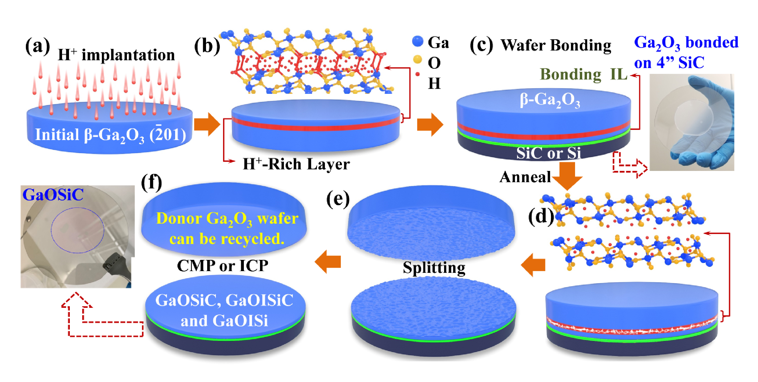
Figure 1:Using the "ion knife" intelligent stripping and transferring technology to process high thermal conductivity substrate heterointegration β-Ga2O3 wafer [IEDM, 2019: 12.5. 1-12.5. 4]
From 2020 to 2021, Professor Han Genquan's team overcame the complex device preparation process, innovated and realized the super crystal valve based on n-Ga2O3/p-NiOx heterostructure (see Figure 3), effectively improving the power quality factor of the device. The relevant results were published at the IEDM conference in 2021.
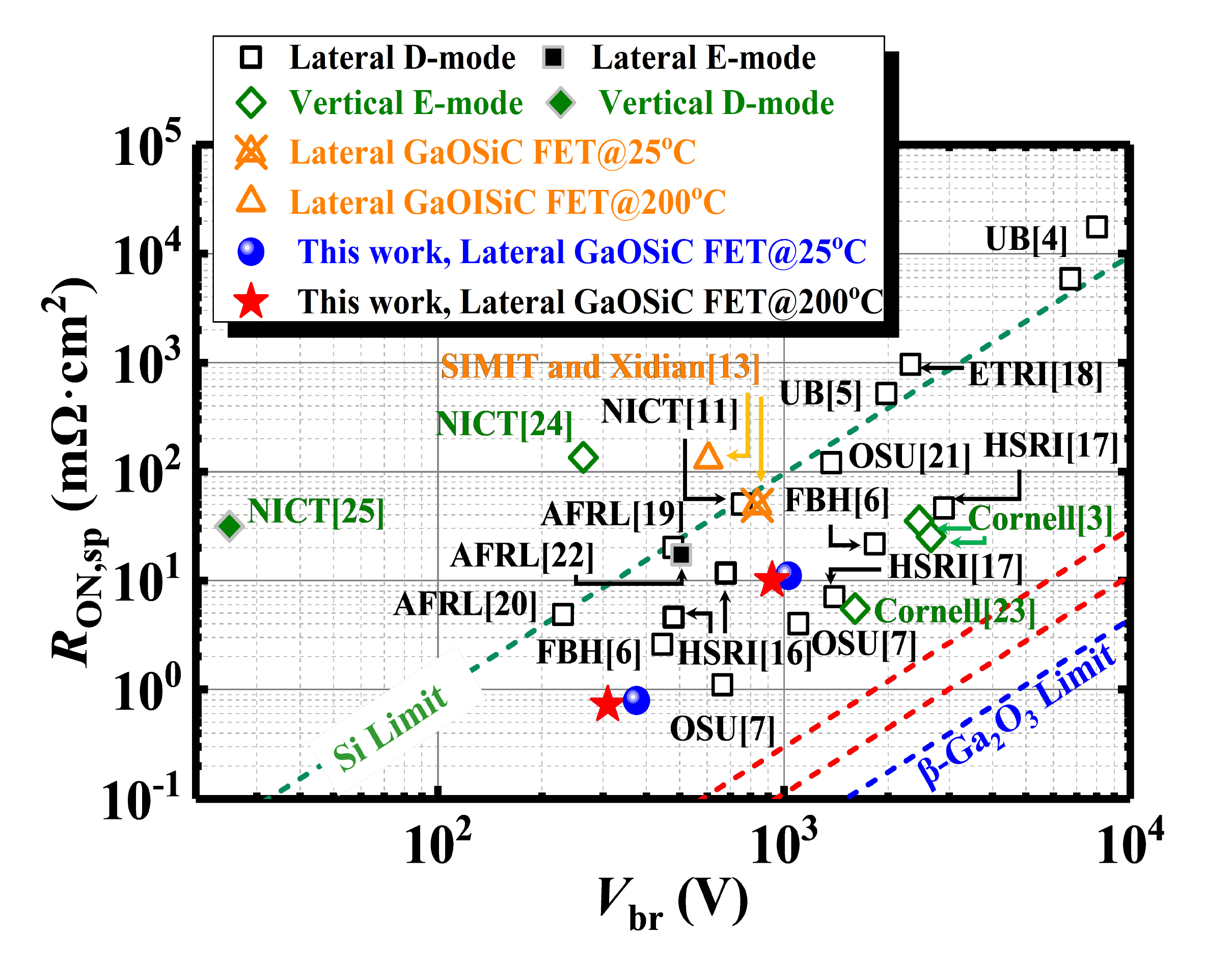
Figure 2:Ga2O3 heterostructure integrated transistor on SiC substrate, whose power quality factor is stable at 100 MW/cm2 in the range of room temperature to 200℃[IEEE TED, 69 (4), 2022: 1945-1949]
From 2020 to 2021, Professor Han Genquan's team overcame the complex device preparation process, innovated and realized the super crystal valve based on n-Ga2O3/p-NiOx heterostructure (see Figure 4), effectively improving the power quality factor of the device. The relevant results were published at the IEDM conference in 2021.
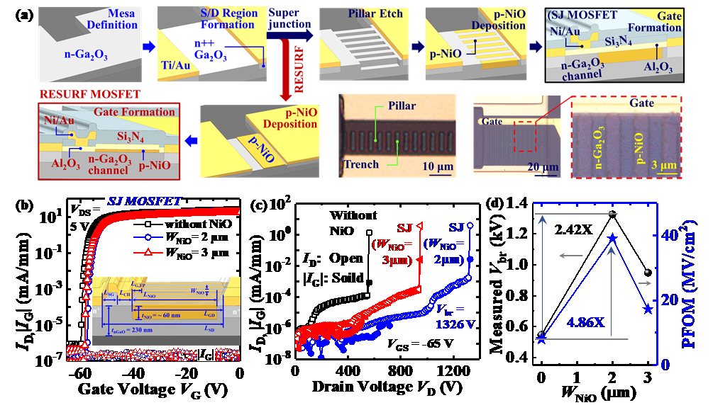
Figure 3:Preparation process of Ga2O3 MOSFETs with RESURF and SJ structures [IEDM, 2021: 36.5.1 - 36.5.4]
With its excellent material properties, Ga2O3 has become a typical representative of ultra wide band-gap semiconductors, and is regarded as one of the ideal materials for the next generation of power and RF devices. It has great potential application value in the field of high voltage resistance, high power and low energy consumption. Its related technology is one of the key technical highlights that many countries are competing for.
Message from the expert
The team will continue to carry out in-depth optimization of existing technologies and development of new technologies for Ga2O3 power and RF devices, and is committed to solving key technical problems in Ga2O3 devices to achieve high-performance Ga2O3 devices.
