Paper Sharing
【Member Papers】Radiation Effects of 500 MeV Kr⁺ ions on NiO/β-Ga₂O₃ heterojunction diodes
日期:2025-08-01阅读:630
Researchers from the Xi’an Jiaotong University have published a dissertation titled "Radiation Effects of 500 MeV Kr+ ions on NiO/β-Ga2O3 heterojunction diodes" in IEEE Transactions on Nuclear Science.
Project Support
This work was supported in part by Guangdong-Hong Kong Technology Cooperation Funding Scheme under Grant 2023A0505010012, in part by the Steady Support Fund for the National Key Laboratory under Grant JBSY252800260, in part by the National Natural Science Foundation of China under Grant 62204198 and Grant 12305299, and in part by the Fundamental Research Funds of the State Key Laboratory of Wide Bandgap Semiconductor Devices and Integrated Technology under Grant 2413S121.
Background
Beta-phase gallium oxide (β-Ga2O3) is gaining attention due to the ultra-wide bandgap (∼4.9 eV), high critical breakdown field of 8 MV/cm, and its availability in the form of melt-grown single crystals and epitaxial layers. At present, β-Ga2O3-based devices, such as Schottky barrier diodes (SBDs), heterojunction diodes (HJDs), and metal-oxide-semiconductor field-effect transistors (MOSFETs), are being developed for applications in high-power electronics, photodetectors, and radiation detectors.
Although β-Ga2O3-based devices exhibit excellent theoretical radiation resistance attributed to their wide bandgap characteristics, their applications in high-radiation environments, including aerospace and nuclear reactors, remain challenging. High-energy heavy ions are a significant source of cosmic radiation that can induce displacement damage and ionizing effects, adversely affecting device performance. Therefore, understanding the degradation mechanisms of β-Ga2O3-based devices under heavy-ion irradiation is critical for their reliable application in space.
Abstract
This study investigates the in situ radiation effects on NiO/beta-phase gallium oxide (β-Ga2O3) heterojunction diodes (HJDs) under 500 MeV Kr+ ions’ irradiation, with a fluence of 1×108 cm−2 at −200 V. The statistical results show that both the forward conductive and reverse blocking characteristics of the HJDs were degraded after the irradiation of Kr+ ions. Associated with the analysis of current-voltage characteristics and the stopping and range of ions in matter (SRIM) simulation results, the performance degradations were attributed to the vacancies induced by Kr+ ions’ radiation in the β-Ga2O3 material. On the one hand, the Kr+ radiation-induced vacancies reduced the net carrier concentration of the β-Ga2O3 and increased the generation-recombination current, leading to increased specificon-resistance and ideality factor of the irradiated HJDs. On the other hand, an oxygen di-vacancies-related trap, set at 1.07 ± 0.01 eV below the conduction band, was involved after Kr+ ions’ radiation, which enhanced the Poole-Frenkel (PF) emission process, dominating the higher leakage current of the irradiated HJDs beyond −300 V. These results provide valuable insights into the radiation damage and performance degradation mechanisms in β-Ga2O3-based devices for space applications.
Conclusion
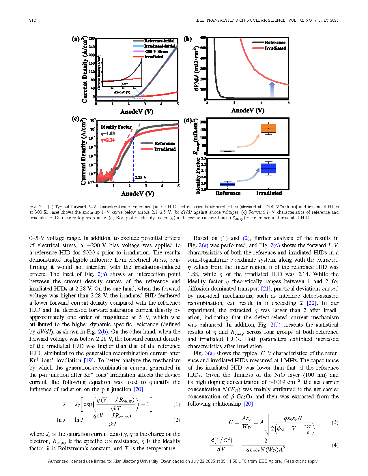
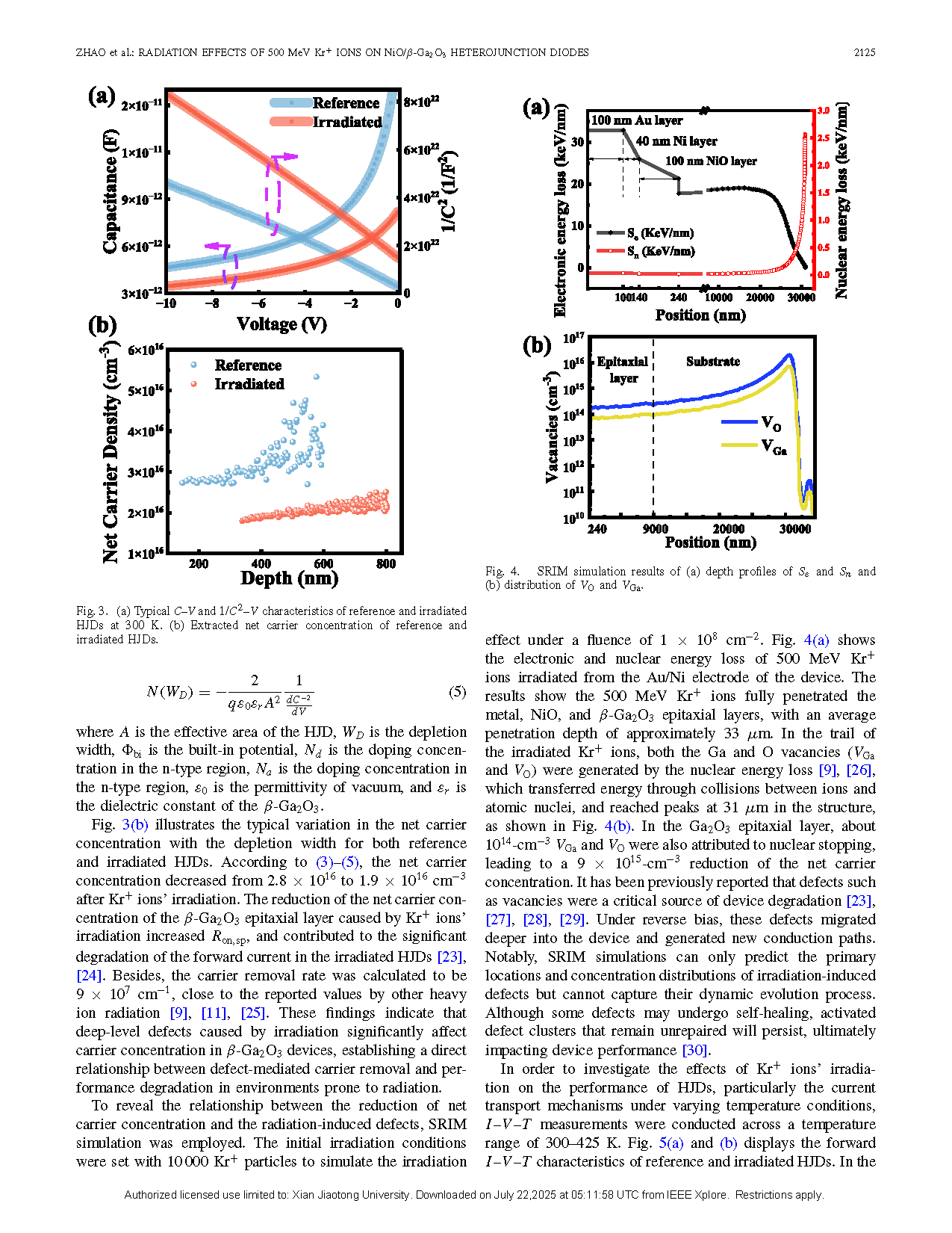
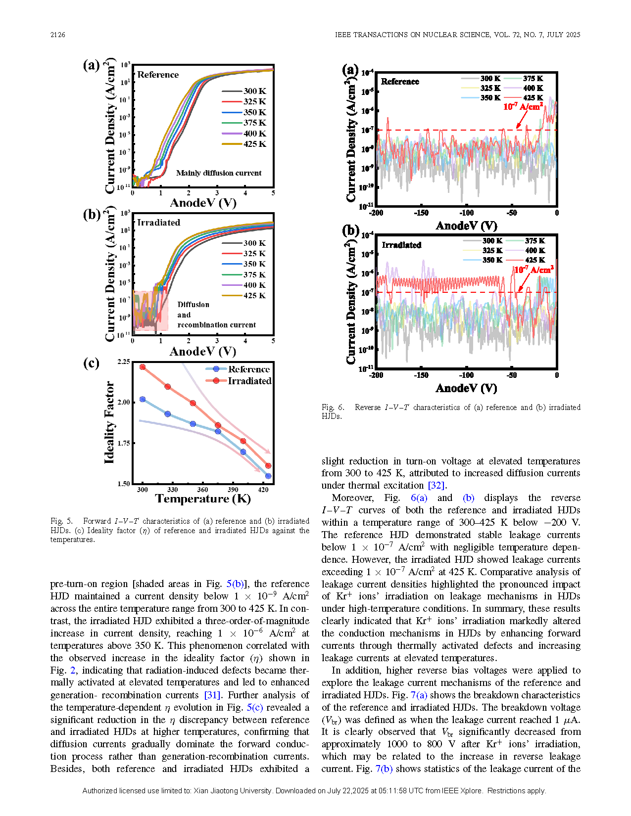
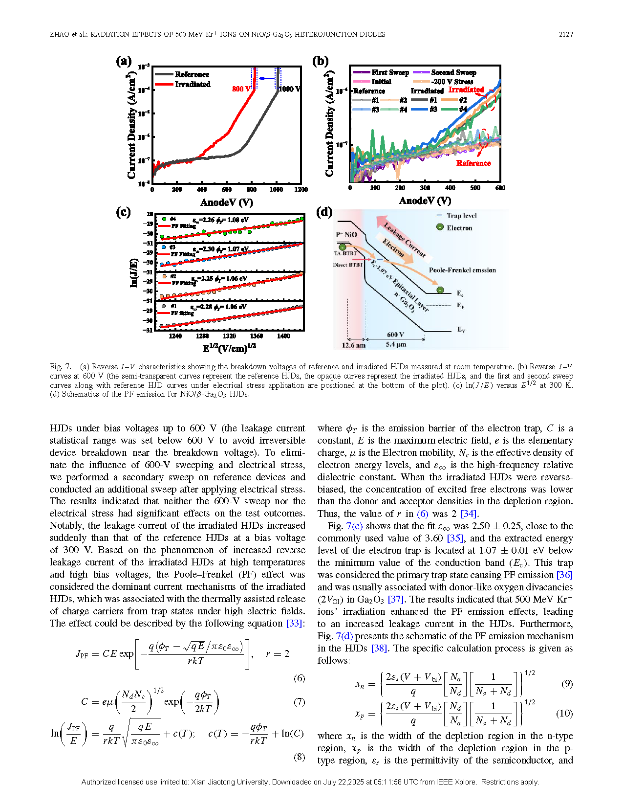
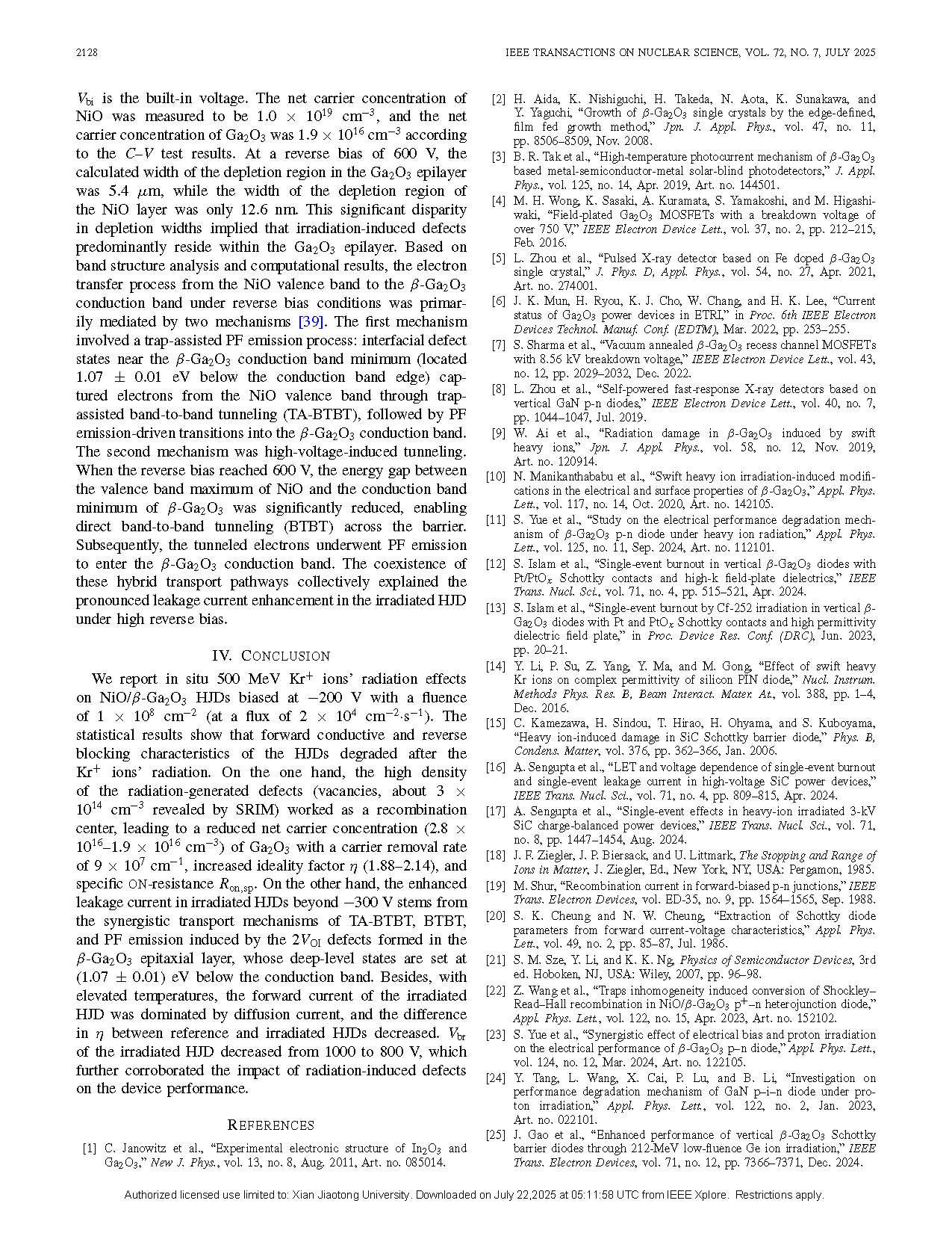
We report in situ 500 MeV Kr+ ions’ radiation effects on NiO/β-Ga2O3 HJDs biased at −200 V with a fluence of 1 × 108 cm−2 (at a flux of 2 × 104 cm−2 ·s −1). The statistical results show that forward conductive and reverse blocking characteristics of the HJDs degraded after the Kr+ ions’ radiation. On the one hand, the high density of the radiation-generated defects (vacancies, about 3 × 1014 cm−3 revealed by SRIM) worked as a recombination center, leading to a reduced net carrier concentration (2.8 × 10¹⁶–1.9 × 1016 cm−3) of Ga2O3 with a carrier removal rate of 9 × 107 cm−1, increased ideality factor η (1.88–2.14), and specific ON-resistance Ron,sp. On the other hand, the enhanced leakage current in irradiated HJDs beyond −300 V stems from the synergistic transport mechanisms of TA-BTBT, BTBT, and PF emission induced by the 2VOI defects formed in the β-Ga2O3 epitaxial layer, whose deep-level states are set at (1.07 ± 0.01) eV below the conduction band. Besides, with elevated temperatures, the forward current of the irradiated HJD was dominated by diffusion current, and the difference in η between reference and irradiated HJDs decreased. Vbr of the irradiated HJD decreased from 1000 to 800 V, which further corroborated the impact of radiation-induced defects on the device performance.
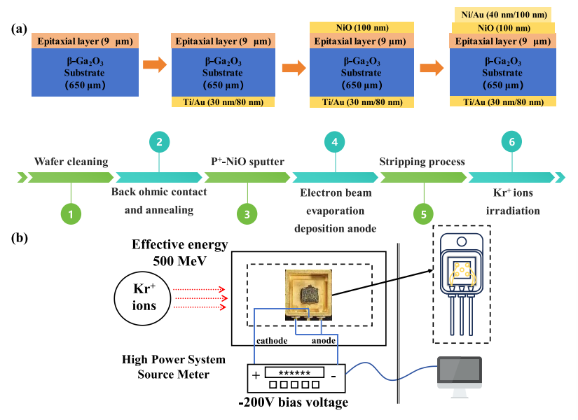
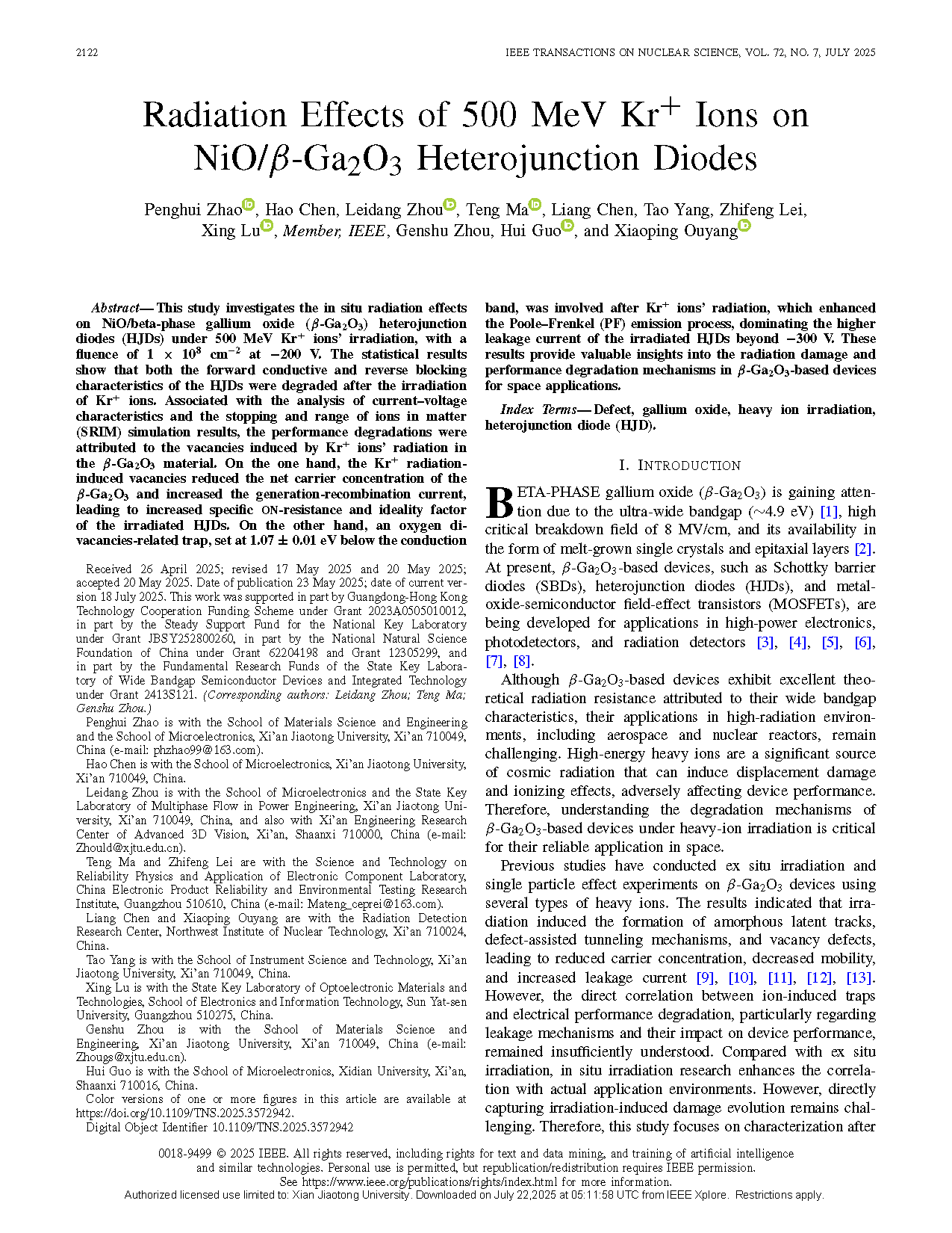
Fig. 1. (a) Preparation process of NiO/β-Ga2O3 HJDs. (b) Schematic of in situ irradiation experiment.
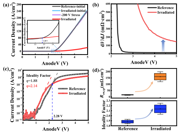
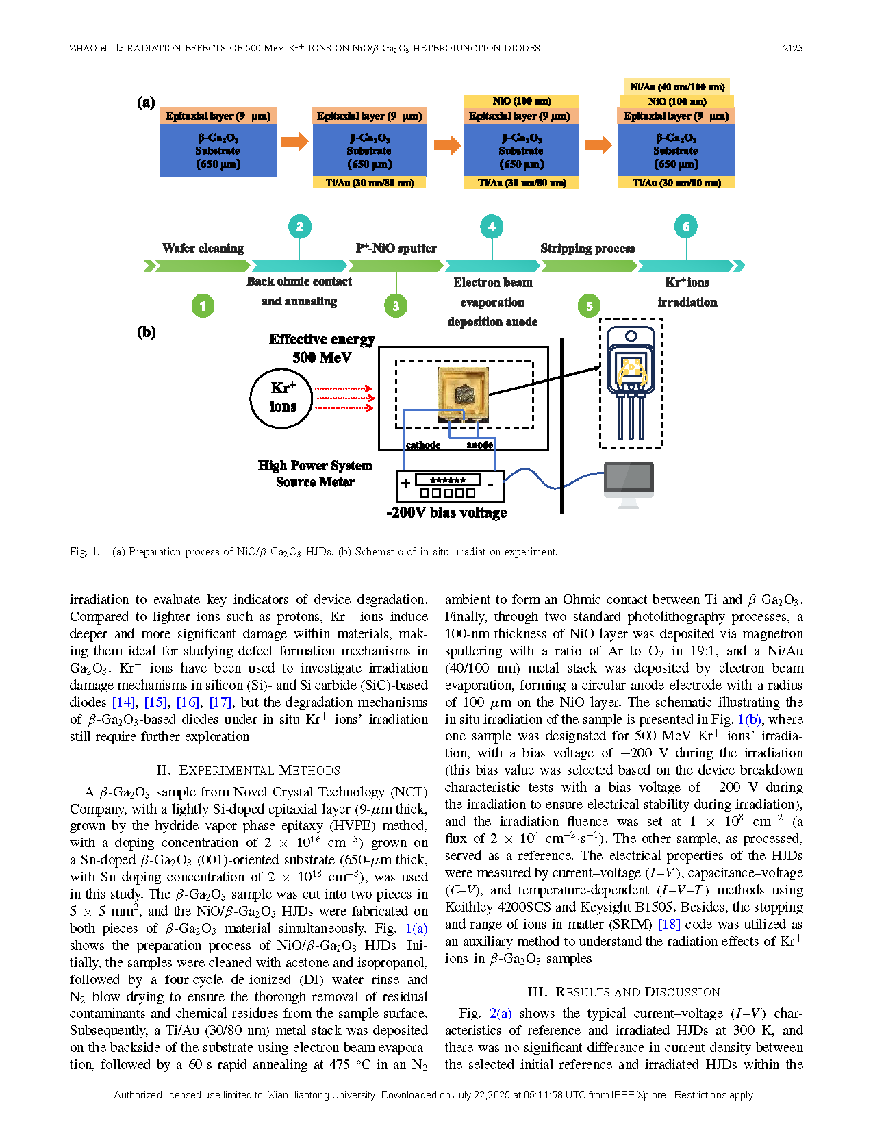
Fig. 2. (a) Typical forward I –V characteristics of reference [initial HJD and electrically stressed HJDs (stressed at −200 V/5000 s)] and irradiated HJDs at 300 K; inset shows the zoom-up I –V curve below across 2.1–2.5 V. (b) dV/dJ against anode voltages. (c) Forward I –V characteristics of reference and irradiated HJDs in semi-log coordinate. (d) Box plot of ideality factor (η) and specific ON-resistance (Ron,sp) of reference and irradiated HJD.
DOI:
doi.org/10.1109/TNS.2025.3572942