


Discover
【Knowledge Discover】Towards Gallium Oxide Power Electronics: Opening a New Chapter of Ultra-Wide Bandgap
日期:2025-08-01阅读:2533
Introduction
Currently, silicon (Si) -based power electronic devices are widely used in various power conversion applications. However, with the acceleration of the global electrification process and the demand for power systems with higher efficiency and greater power density intensifies, the limitations of silicon-based devices in terms of voltage handling capacity, switching speed, and system efficiency have become increasingly prominent. The low bandgap characteristics of traditional silicon have become an insurmountable bottleneck, particularly in where ultra-high voltage power conversion above 20kV is required. In addition, silicon-based devices generate a large amount of heat during operation, much of which needs to be dissipated through cooling measures, which not only causes energy waste but also drives up the cost of the cooling system, and their operating temperature and switching frequency are also strictly limited.
To break through these technical bottlenecks, research in the semiconductor field is gradually shifting towards wide bandgap (WBG) semiconductors such as Silicon Carbide (SiC) and Gallium Nitride (GaN). SiC has developed into a mature commercial power electronics technology platform, and sic-based inverters can achieve higher switching frequencies in smaller sizes, significantly outperforming silicon-based devices. However, even for SiC, it is difficult to increase the switching frequency of power converters above 10 kHz without sacrificing efficiency when the voltage exceeds 10 kV.
Against this backdrop, Gallium Oxide (Ga₂O₃) ultra-wide bandgap (UWBG) semiconductor materials are rapidly emerging as strong competitors for the next generation of power electronic devices. The bandgap width of Gallium Oxide is as high as approximately 4.85 eV. This ultra-wide bandgap characteristic endows it with material advantages far exceeding those of SiC and GaN, making it show great potential in achieving extremely high withstand voltage and efficient power electronic devices. In 2012, the successful demonstration of the first Gallium Oxide transistor marked a breakthrough for this emerging material in the field of power electronics. Although its commercialization process still faces challenges, Gallium Oxide, with its unique advantages, is becoming a focus of attention in the industry.
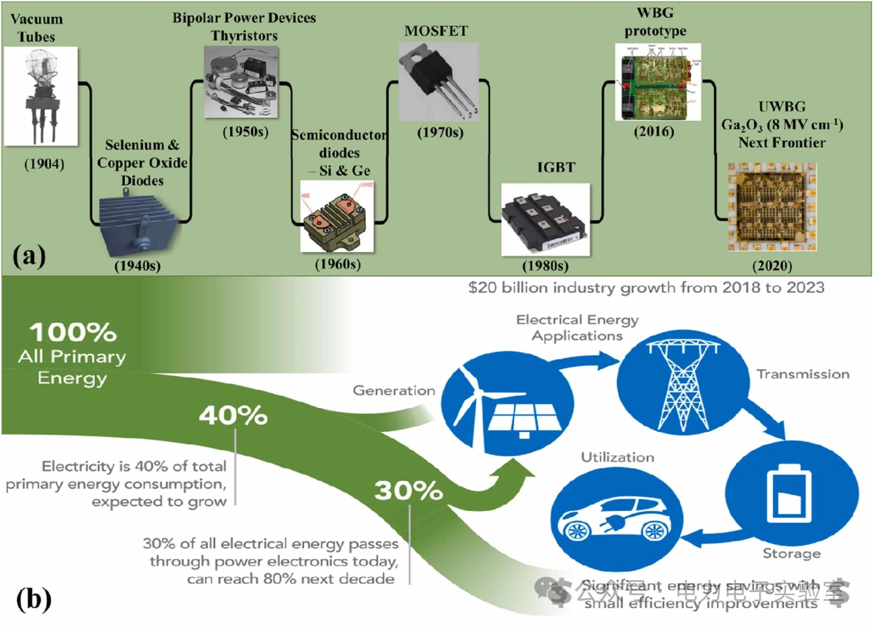
Figure 1 Evolution of power electronic devices and power distribution
The Core Advantages of Gallium Oxide
Gallium Oxide (Ga₂O₃) stands out among numerous new materials due to its unique crystal growth advantages and outstanding intrinsic material properties, which together form a solid foundation for its advancement into the future field of power electronics. It is worth mentioning that Gallium Oxide has multiple crystal structures (i.e., polycrystalline forms), including α-Ga₂O₃ (corundum structure), β-Ga₂O₃ (monoclinic system), γ-Ga₂O₃ (cubic spinel), δ-Ga₂O₃ (cubic), and ε-Ga₂O₃ (hexagonal). Among them, β-Ga₂O₃ of the monoclonal crystal system is currently the most stable, most deeply studied and most suitable "phase" for power electronics applications. Therefore, this article mainly discusses its characteristics and progress.
1 Unique Crystal Growth Advantages
Unlike other wide bandgap semiconductors, such as SiC and GaN, which face challenges in substrate growth, β-Ga2O3 can be mass-produced using more cost-effective melt growth methods like the mature silicon industry, such as EFG (Edge-Definde Film-Fed Growth method), CZ (Czochralski method), etc. This has enabled it to produce large-sized, high-quality single-crystal substrates, with commercial supply of 4-inch wafers already achieved and expected to reach 6-inch by 2027. This significant low-cost advantage is the key factor driving the industrialization of Gallium Oxide power electronics technology.
2 Controllable N-Type Conductivity
In terms of N-type conductivity, Gallium Oxide demonstrates excellent control ability. The presence of shallow-level donors and acceptors (charged impurities) has long plagued all ultra-wide bandgap (UWBG) semiconductors because the wider the bandgap, the farther the external impurities are usually from the conduction band (or valence band). However, for Gallium Oxide (Ga₂O₃), silicon is an efficient external shallow donor dopant, enabling it to achieve a very wide range of controllable conductivity from less than 1014 cm-3 to more than 1020 cm-3. This wide-range and precisely tunable N-type conductivity is crucial for the design and manufacture of power electronic devices with various properties, such as different withstand voltage and different on-resistances. For example, different regions of the device (such as the high-resistance drift region and the low-resistance ohmic contact region) can obtain precise conductivities as required.
3 Outstanding Material Properties
In addition to the above-mentioned growth and doping advantages, Gallium Oxide also possesses remarkable intrinsic material properties.
- Its ultra-wide bandgap of up to 4.6-4.9 eV gives it a theoretical breakdown electric field strength of up to approximately 8MV/cm, far exceeding that of Si, SiC and GaN. This means that Gallium Oxide devices can withstand higher voltages while achieving smaller chip sizes, significantly enhancing power density.
- In addition, Gallium Oxide also features extremely high thermal stability, with a melting point as high as 1700°C, as well as excellent chemical stability, enabling it to operate reliably in harsh environments such as high temperatures. Its ultra-wide bandgap also gives it excellent radiation resistance, making it have unique application potential in high-radiation environments such as space and nuclear reactors.
- In terms of on-resistance, Gallium Oxide materials themselves also have the theoretical potential to achieve extremely low on-resistance, which is crucial for further reducing the energy loss of devices in the on state.
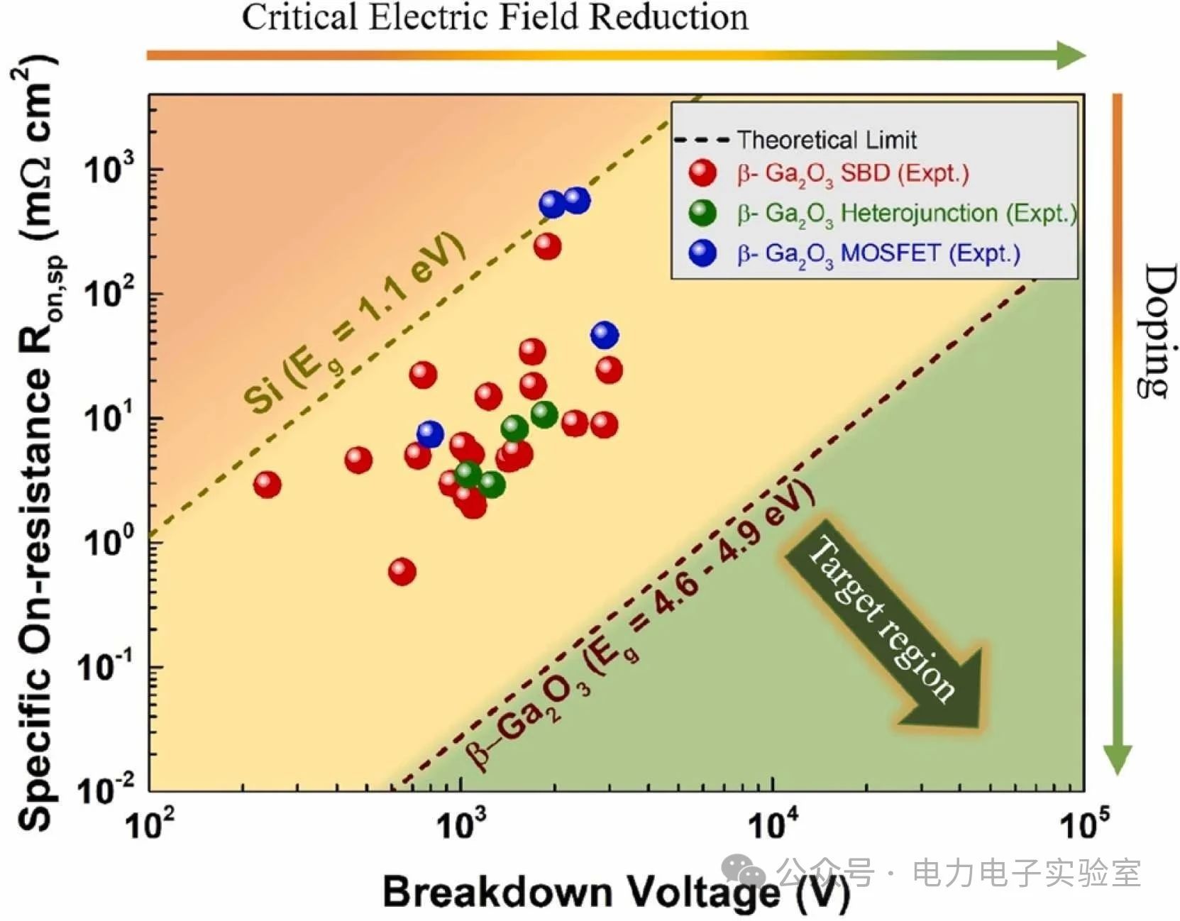
Figure 2. Diagram of β-Ga2O3 on-resistance versus breakdown voltage
Architecture and Progress of Gallium Oxide Power Electronic Devices
While breakthroughs have been made in materials and crystal growth, the development of Gallium Oxide power electronic devices is also advancing rapidly. Researchers are actively exploring various device architectures to fully leverage the superior performance of Gallium Oxide.
1 A Diverse Exploration of Device Architectures
● Vertical Field-Effect Transistors (such as FinFET) : Theoretically, vertical devices can maximize the utilization of the high breakdown electric field advantage of Gallium Oxide to achieve extremely high withstand voltage capabilities. For example, the vertical β-Ga2O3 FinFET, which has been successfully demonstrated, can block voltages up to 4.2 kV. However, such devices are relatively sensitive to the spread defect in thick epitaxial layers, which to some extent affects the stability and repeatability of their performance.
● Lateral Heterojunction Field-Effect Transistors (HFET) : Compared with vertical structures, lateral HFET shows great potential in achieving faster switching speeds and higher efficiency. The power performance of the device can be further enhanced by introducing ternary alloys such as β-(AlxGa1-x)3O2, for example, achieving higher two-dimensional electron gas (2DEG) density. This structure holds great promise for power management and RF applications that require high-frequency switching.
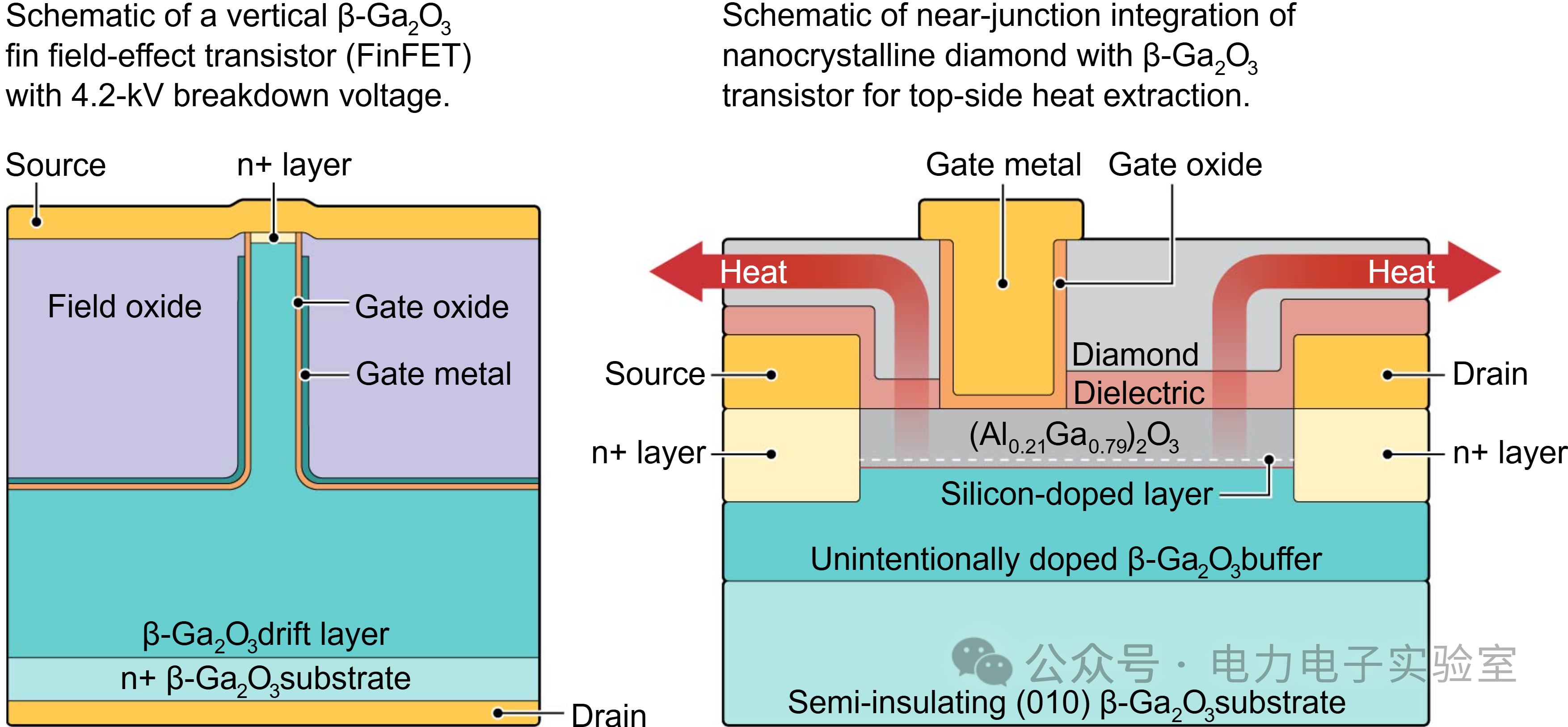
Figure 3. Different types of Ga2O3 FET structures
2 Commercial Progress and Types of Diodes
1). Schottky Barrier Diode (SBD)
Among various Gallium Oxide power electronic devices, the Schottky Barrier Diode is currently the most mature type of device and is widely expected by the industry to be among the first to be commercialized. Its structure is relatively simple and the preparation process is quite feasible, which enables it to achieve high-level performance relatively quickly.
● Outstanding performance: Gallium Oxide SBDS have achieved a breakdown voltage of over 3 kV, and their BFOM (a key indicator for measuring the overall performance of devices) has also approached 1 GW/cm², demonstrating potential to rival SiC diodes. These outstanding performances give it a significant advantage in high-voltage, high-frequency switching applications.
● Key technologies: To fully utilize the extremely high breakdown electric field of Gallium Oxide and effectively suppress the edge electric field concentration and leakage current of the device under high voltage, researchers have developed a variety of advanced edge terminal technologies. This includes field plates, trench MOS SBD, double-layer media, protection rings and floating metal rings, etc. The application of these technologies is crucial for enhancing the withstand voltage capacity and overall reliability of Gallium Oxide SBDS.
2). Advances in Other Diode Types
In addition to SBD, researchers are also actively exploring other Gallium Oxide diode structures:
● Heterojunction Schottky Diode: This usually refers to the introduction of a heterointerface in an SBD structure to further optimize contact characteristics or electric field distribution, thereby enhancing device performance.
● P-N Heterojunction Diode: The development of this type of diode mainly addresses the fundamental challenge of the lack of P-type conductivity of Gallium Oxide itself. By combining Gallium Oxide (N-type) with another P-type semiconductor material (such as NiO, GaN, etc.) to form a heterojunction, devices similar to traditional PN junctions can be constructed. Although this type of diode is of crucial significance for the realization of Gallium Oxide bipolar devices, its technological maturity is still inferior to that of SBD at present.
3). Commercial Outlook
It is precisely because of the relative maturity of SBD technology that the industry generally predicts that if it can continuously receive investment and R&D support, Gallium Oxide power diodes are expected to be the first to enter commercial application within the next ten years.
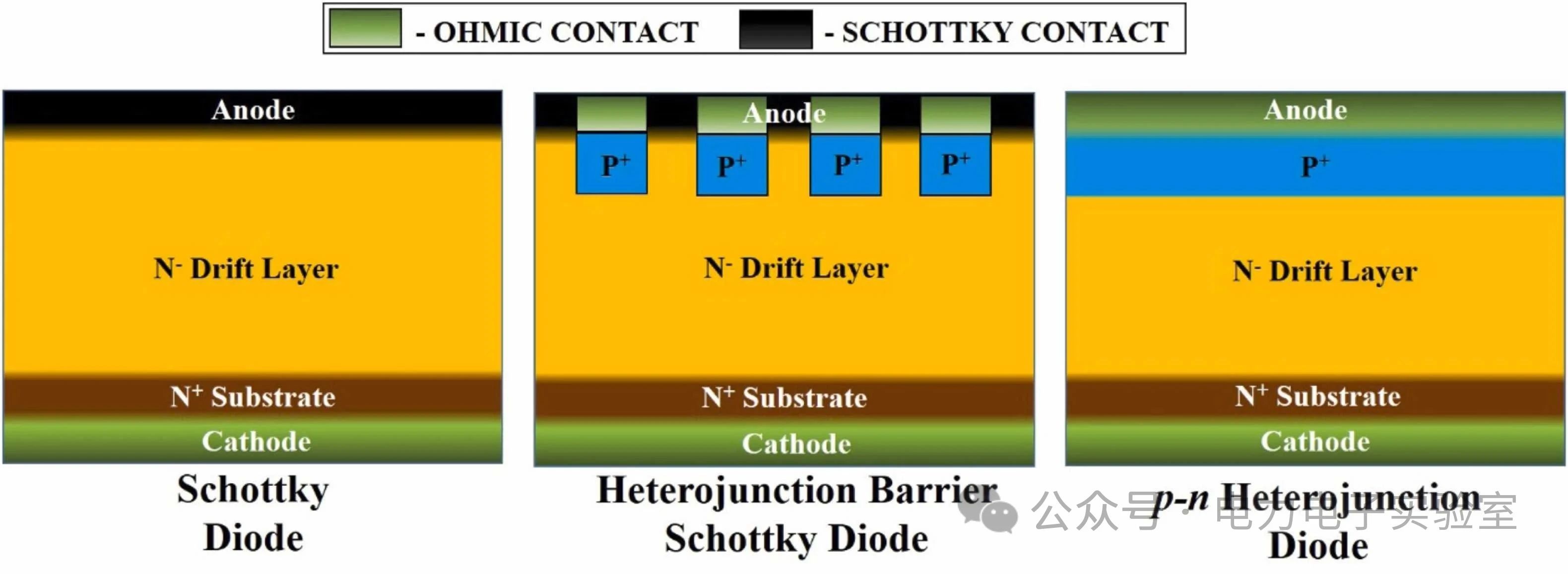
Figure 4. Different types of Ga2O3 diode structures
Key Challenges and Countermeasures for Gallium Oxide
Although Gallium Oxide has a promising future as a next-generation power electronic material, its commercial application still faces some key challenges. A thorough understanding and effective solution to these problems is the inevitable path to promoting Gallium Oxide technology from the laboratory to the market.
1 The Absence of P-Type Conductivity
This is one of the greatest challenges that Gallium Oxide, as a semiconductor material, faces. Due to its unique band structure, especially the flat valence band structure, the effective mass of the holes is very high, as shown in Figure 5(a). This characteristic makes the holes prone to form local polarons and self-trapping effects, resulting in the material itself not having stable P-type conductivity. This fundamental limitation hinders the realization of bipolar devices such as IGBTs and the ideal PN junction, which is a fundamental component of many complex power electronic devices such as PN diodes, MOSFETs, and IGBTs.
Exploring heterojunction integration is a major and effective approach to addressing the absence of P-type conductivity at present. For instance, the NiO Gallium Oxide p-n heterojunction has been successfully demonstrated and can be used to achieve effective electric field management and charge balance. In the future, research will focus more on heterointegration with P-type wide bandgap semiconductors, such as GaN or AlN, in order to construct high-performance p-n junction devices.
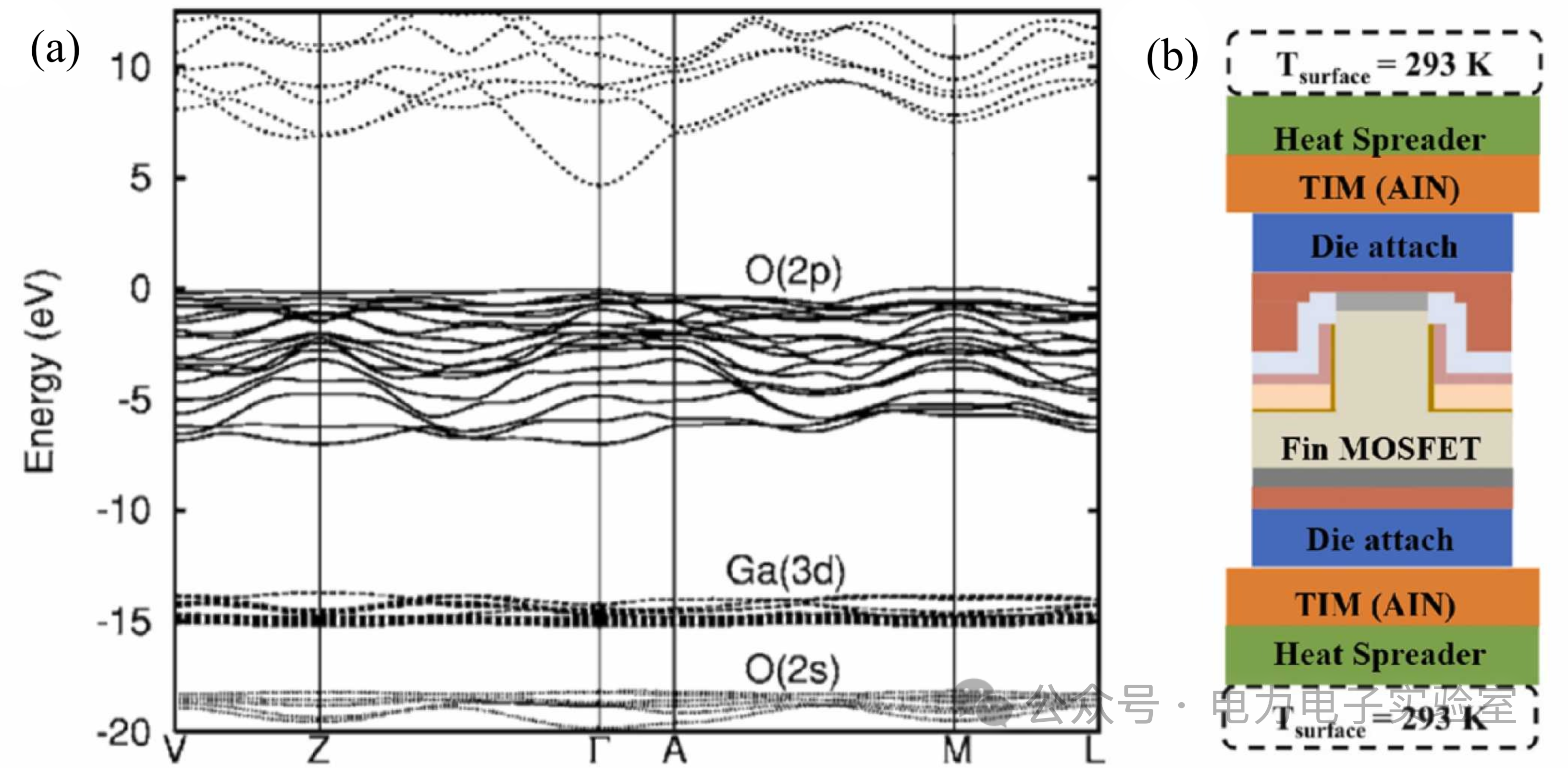
Figure 5. (a). Ga2O3’s valence band structure (b). Schematic diagram of double-sided cooling
2 Low Thermal Conductivity
The intrinsic thermal conductivity of Gallium Oxide is extremely low, typically only 11 to 27 W m-1 K-1, which is much lower than that of SiC and GaN. Effective thermal management is crucial for high power density devices, otherwise it can lead to device overheating, performance degradation or even failure. The low thermal conductivity of Gallium Oxide poses more severe challenges in heat dissipation than GaN devices.
To address this issue, researchers are exploring countermeasures from multiple perspectives. One feasible approach is to use top, bottom, and double-sided cooling configurations to assist in heat dissipation, as shown in the double-sided cooling structure in Figure 5(b). Devices can also be mounted on high thermal conductivity substrates such as synthetic diamond and standard copper-tungsten alloys when packaged for better heat dissipation. Another approach is to reduce the total thermal resistance of the device. Another method is to reduce the total thermal resistance of the device by using a thin and highly thermally conductive substrate, such as synthetic diamond, for heteroepitaxial growth. Just as commercial GaN devices utilize the high thermal conductivity of SiC substrates, synthetic diamond, due to its four times higher thermal conductivity than copper, can be the best feasible choice for Gallium Oxide. In addition, a more promising option is heterointegration with high thermal conductivity wide bandgap semiconductors such as SiC, GaN or even diamond. For example, bonding or integrating nanocrystalline diamond into a lateral transistor has been proven to significantly improve heat dissipation efficiency. The researchers also conducted theoretical simulations of certain device topologies by using electrode contacts and dielectric fillers to dissipate heat to the heat sink, and the results of the theoretical simulations were promising, a method currently applied to commercial GaAs heterojunction bipolar transistors. In conclusion, through appropriate device engineering, it is expected to solve the problem of low thermal conductivity of Gallium Oxide.
3 Defect Control and Reliability
As the thickness of the Gallium Oxide epitaxial layer increases to meet the requirements of high-voltage devices, the point defect (such as oxygen vacancies and their complexes) that may occur and extended defect (such as dislocations) remain the key factors restricting the performance, stability and size of the devices. These defect can lead to an increase in leakage current, a decrease in breakdown voltage, and long-term reliability issues of the device.
In the coming years, a thorough understanding, precise characterization and effective control of these defect will be the core tasks for commercializing high-voltage Gallium Oxide devices. At present, the accumulation of reliability data on Gallium Oxide devices is still in its early stage, and a large amount of long-term testing and research are needed to establish industry standards. In the coming years, a thorough understanding, precise characterization and effective control of these defects will be the core tasks for commercializing high-voltage Gallium Oxide devices. At present, the accumulation of reliability data on Gallium Oxide devices is still in its early stage, and a large amount of long-term testing and research are needed to establish industry standards.
4 Development of Specialized Manufacturing Processes
Traditional semiconductor manufacturing processes, especially dry etching that relies on plasma etching, may introduce defect and damage on the surface of Gallium Oxide, thereby affecting the performance and reliability of devices.
It is of vital importance to develop a unique low-damage manufacturing process for Gallium Oxide. For instance, researchers are actively exploring alternative solutions such as wet etching and gas phase etching to avoid surface damage caused by plasma etching. Also, breakthroughs in selective ion implantation technology are crucial, which can precisely pattern conductive and insulating regions in the substrate or epitaxial layer, thereby enhancing device performance and reliability.
Outlook: Investment, Innovation and System-Level Applications
Gallium Oxide, with its unique material advantages and significant progress in device development, is gradually moving from academic research to industrial application. Looking ahead, continuous investment, unremitting technological innovation and deep integration at the system level will jointly drive Gallium Oxide power electronics technology towards a broader application stage.
1 Continuous Investment and Industrial Ecosystem Improvement
With the increasing potential of Gallium Oxide as the next-generation power electronic material, global R&D investment and industrial attention have continued to rise. Major economies and industry giants are actively laying out, and the improvement and maturity of the entire industrial chain, from crystal growth, epitaxial preparation, device design to packaging and testing, is the key to achieving large-scale commercialization in the next decade. It is expected that under the continuous investment drive, initial products such as Gallium Oxide power diodes will be the first to enter the market.
2 Driven by Diverse Technological Innovations
Innovations in the field of Gallium Oxide in the future will be multi-dimensional. At the material level, the pursuit of large-sized, low defect and high uniformity substrates will continue. Meanwhile, heterogeneous integration technology of high thermal conductivity substrates (such as the combination with diamond and SiC) will be an important direction for enhancing the heat dissipation capacity of devices. At the device level, in addition to the continuous optimization of SBD and HFET performance, breakthroughs in p-n heterojunctions will unlock more complex bipolar devices and further expand their application range. In addition, the development of dedicated low-damage manufacturing processes and the in-depth study of device reliability under conditions such as high temperature, high power, and extreme environments will be at the core of future technological breakthroughs.
3 Broad System-Level Application Prospects
The extremely high breakdown electric field strength and low on-resistance potential of Gallium Oxide make it an ideal choice for realizing ultra-high voltage (>20 kV) power conversion electronic devices. At the system level, gallium oxide devices are expected to play a key role in the following areas:
● Electric vehicles and rail transit: Improve power conversion efficiency, extend range, reduce system volume and weight.
● Smart grids and renewable energy: Applications in high-voltage direct current (HVDC) transmission, smart substations, wind power, solar inverters, etc., to improve energy conversion efficiency and grid stability.
● Industrial power and data centers: Meet the demands of high-power, high-efficiency power management and reduce energy consumption.
● Aerospace and Defense: Reliable operation in extreme environments thanks to its excellent radiation resistance and high-temperature properties.
To sum up, Gallium Oxide is at a critical juncture of transitioning from a "research star" to an "industry mainstay". Despite the challenges, its unique advantages and the joint efforts of the global scientific research and industrial community indicate that it will play an increasingly important role in the future power electronics field and lead a new round of power technology revolution.
Reference
● Tadjer M J. Toward gallium oxide power electronics. Science, 2022, 378(6621): 724-725.
● Kaur D, Ghosh A, Kumar M. A strategic review on gallium oxide based power electronics: Recent progress and future prospects. Materials Today Communications, 2022, 33: 104244.
● Green A J, Speck J, Xing G, et al. β-Gallium oxide power electronics. Apl Materials, 2022, 10(2).
● C. R. Eddy Jr., D. K. Gaskill, Science 324, 1398 (2009).
● M. Higashiwaki, K. Sasaki, A. Kuramata, T. Masui, S. Yamakoshi, Appl. Phys. Lett. 100, 013504 (2012).
● S. J. Pearton et al., Appl. Phys. Rev. 5, 011301 (2018).
● Novel Crystal Technology, Inc., Current commercial β-Ga2O3 wafer suppliers; www.novelcrystal.co.jp/.
● J. A. Spencer et al., Appl. Phys. Rev. 9, 011315 (2022).
● G. Seryogin et al., Appl. Phys. Lett. 117, 262101 (2020).
● J. B. Varley, A. Janotti, C. Franchini, C. G. Van de Walle, Phys. Rev. B 85, 081109 (2012).
● J. Zhang et al., Nat. Commun. 13, 3900 (2022).
● H.-C. Huang, Z. Ren, C. Chan, X. Li, J. Mater. Res. 36, 4756 (2021).
● N. K. Kalarickal et al., Appl. Phys. Lett. 119, 123503 (2021).
● M. J. Tadjer, T. J. Anderson, Eds., Thermal Management of Gallium Nitride Electronics (Elsevier, 2022).
● N. A. Mahadik, R. E. Stahlbush, W. Sung, J. Appl. Phys. 131, 225702 (2022).
● M. D. McCluskey, J. Appl. Phys. 127, 101101 (2020).
● J. Y. Tsao et al., Adv. Electron. Mater. 4, 1600501 (2018).
