Paper Sharing
【Member Papers】C-Band β-Ga₂O₃-on-SiC RF Power MOSFETs With High Output Power Density and Low Microwave Noise Figure
日期:2025-08-04阅读:703
Researchers from the Xidian University have published a dissertation titled "C-Band β-Ga2O3-on-SiC RF Power MOSFETs With High Output Power Density and Low Microwave Noise Figure" in IEEE Transactions on Electron Devices.
Project Support
This work was supported in part by the National Natural Science Foundation of China (NSFC) under Grant 62222407 and Grant 62421005, and in part by Guangdong Basic and Applied Basic Research Foundation with under Grant 2023B1515040024.
Background
Ultra-wide bandgap (UWBG) semiconductor β-Ga2O3 is widely studied as a competitive power device material for next-generation power electronics, due to its bandgap of 4.8 eV, high Baliga’s Figure-of-Merit (B-FOM) as well as high Johnson-FOM (J-FOM). However, it should be noted that the fundamental research is mainly focused on the high voltage power applications, only several reports on the RF performances are available from thousands of published literatures. It is generally accepted that the low electron mobility and extremely low thermal conductivity are major obstacles toward realizing high performance RF power FETs, although the saturation velocity of β-Ga2O3 is 1.5∼2 × 107 cm/s. Consequently, representative record Pout = 1.3 W/mm at f = 5 GHz was only achieved. It seems that there are several bottlenecks that needed to be surmounted in order to take full advantage of high saturation velocity and high critical field of β-Ga2O3 and then open up a new route for β-Ga2O3 research, which is targeted for high-frequency and high-power RF device applications.
Abstract
In this letter, we show that β-Ga2O3-on-SiC RF power metal-oxide-semiconductor field-effect transistors (MOSFETs) can achieve a high output power density (Pout) for C-band applications by implementing a heavily doped channel to reduce channel resistance and a high thermal conductivity SiC substrate to enhance heat dissipation. By doing so, β-Ga2O3-on-SiC RF MOSFETs demonstrate a drain current density (ID) of 730 mA/mm and peak transconductance (gm) of 81 mS/mm. As a result, cut-off frequency (fT) and maximum oscillation frequency (fmax) of 19.2 and 35.3 GHz are achieved, respectively. Benefited from the suppressed self-heating effect under high drain bias (VDS) operation condition, the RF power performances with output power density (Pout) =3.5 W/mm at 4 GHz and Pout=3.2 W/mm at 6 GHz are reported. To the best of all the authors’ knowledge, this is the highest Pout at C-Band among all β-Ga2O3 RF power FETs. In addition, this work studies the microwave noise characteristics of the β-Ga2O3 RF MOSFETs at frequency (f) range of 2–15 GHz. The device is able to achieve a low minimum-noise figure (NFmin) of 1.4 dB at 2 GHz and 1.8–2.5 dB at 4–6 GHz. β-Ga2O3 RF power MOSFETs with heavily doped channel and high thermal conductivity substrate verify their great promise for future high power, high frequency, and low noise RF electronics.
Conclusion
In conclusion, we have demonstrated a β-Ga2O3-on-SiC MOSFET with high RF power performances at C-band. A well-controlled current collapse, reduced channel resistance and effectively enhanced heat dissipation are achieved by implementing a heavily doped β-Ga2O3/SiC composite structure. The resultant device exhibits superior performance of a high current density of 730 mA/mm, a peak transconductance of 81 mS/mm, record a Pout = 3.5 W/mm with PAE = 15.1% at 4 GHz and a Pout = 3.2 W/mm with PAE = 7.8% at 6 GHz. Meanwhile, we report the microwave-noise characteristics of oxide RF transistors, highlighting a low NFmin of 1.4 dB at 2 GHz and 1.8–2.5 dB at 4–6 GHz. These results show the great promise of β-Ga2O3-on-SiC RF power MOSFETs for future high-frequency, high-power, and low-noise applications.
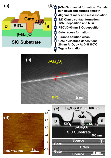
Fig. 1. (a) 3-D cross-sectional schematic view of β-Ga2O3 RF MOSFET on a SiC substrate. (b) Key fabrication process steps of β-Ga2O3-onSiC RF power MOSFETs. (c) HRTEM image of β-Ga2O3/SiC sample. (d) AFM image of the piranha solution treated β-Ga2O3 thin film. (e) Focus ion beam (FIB) cross-sectional image of the device. (f) Top-view scanning electron microscope (SEM) image.
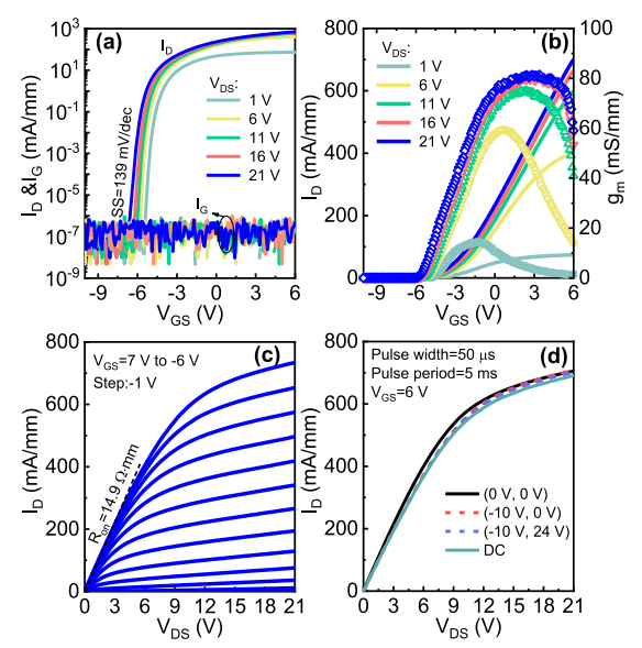
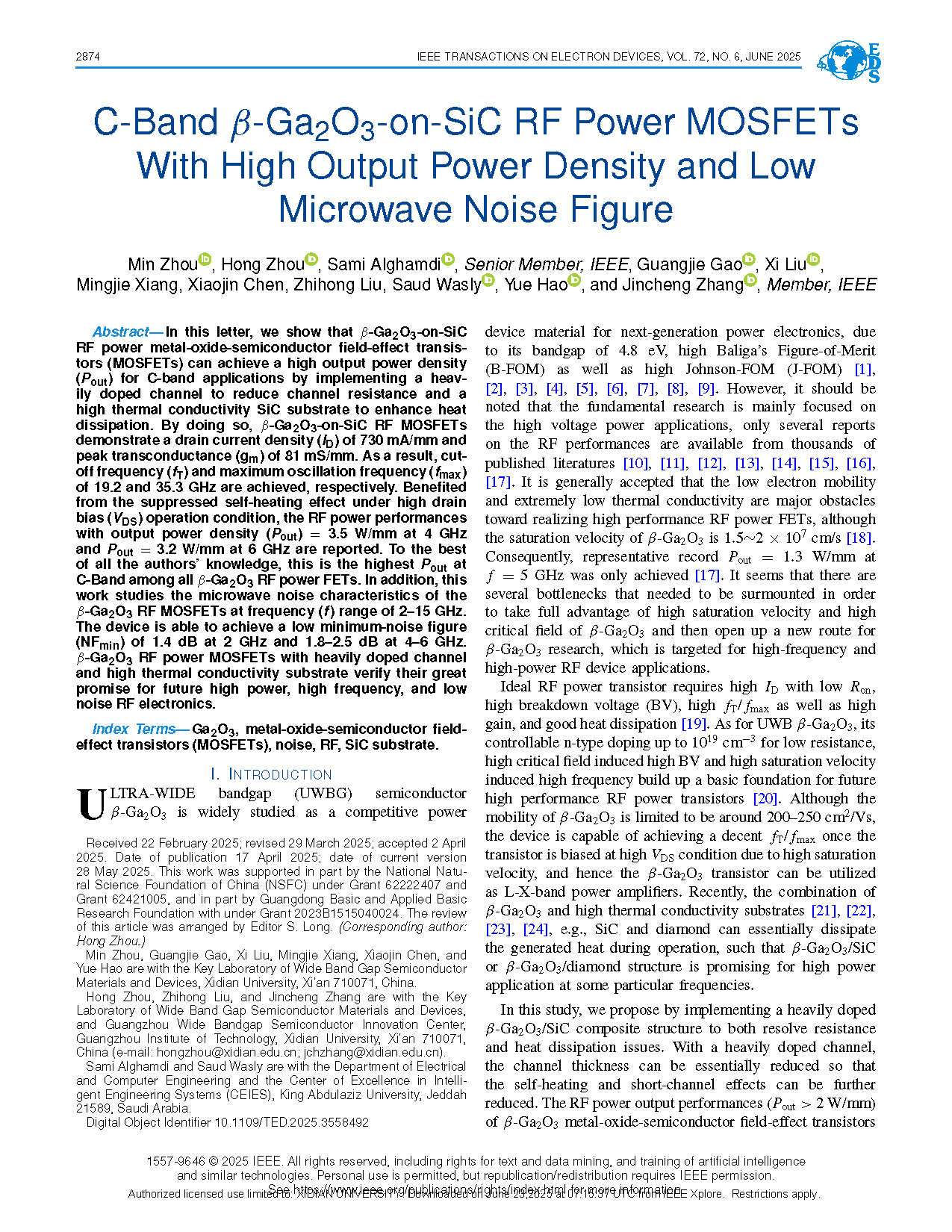
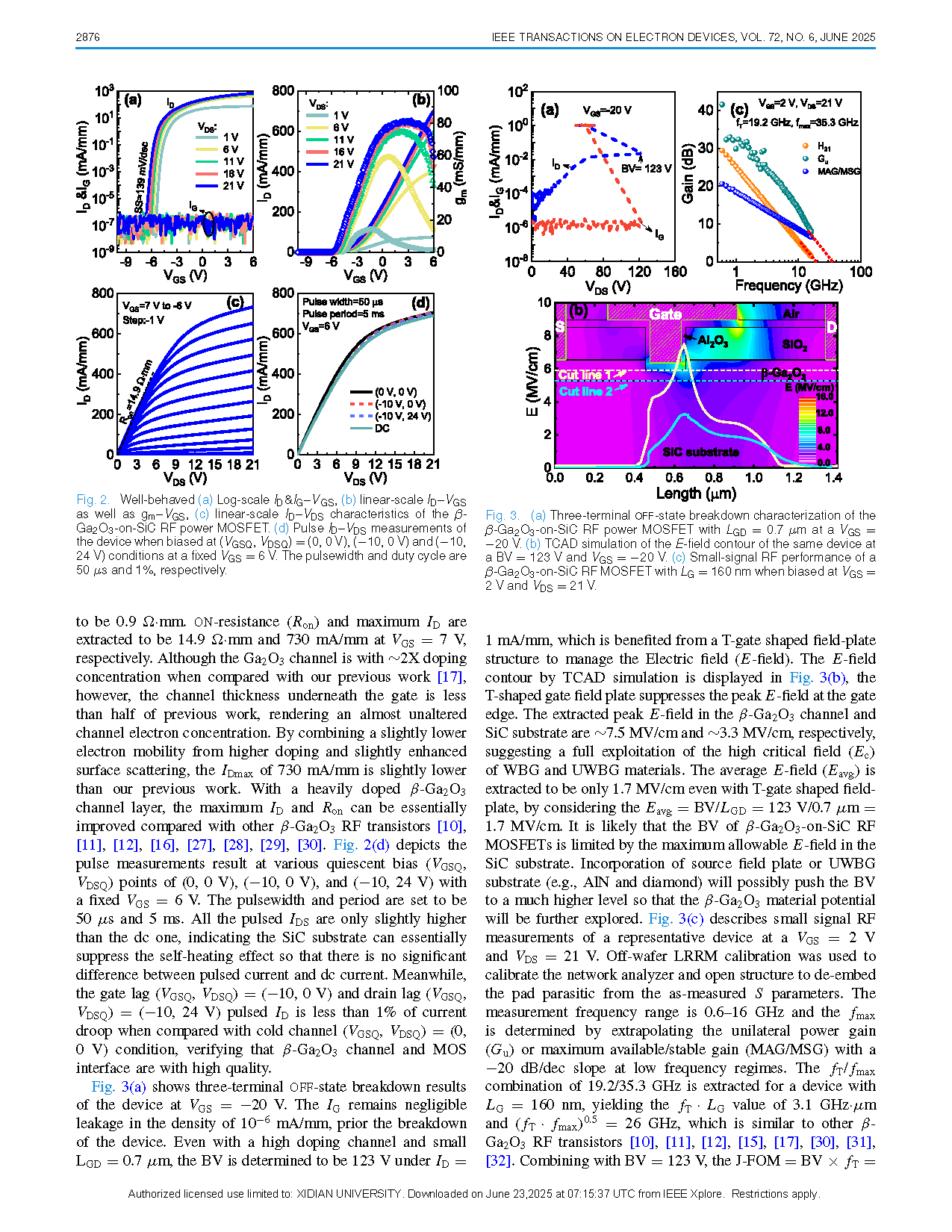
Fig. 2. Well-behaved (a) Log-scale ID&IG–VGS, (b) linear-scale ID–VGS as well as gm–VGS, (c) linear-scale ID–VDS characteristics of the β-Ga2O3-on-SiC RF power MOSFET. (d) Pulse ID–VDS measurements of the device when biased at (VGSQ, VDSQ) = (0, 0 V), (−10, 0 V) and (−10, 24 V) conditions at a fixed VGS = 6 V. The pulsewidth and duty cycle are 50 µs and 1%, respectively.
DOI:
doi.org/10.1109/TED.2025.3558492