


Member Intro
【Member Intro】Fujian Sunwise Semiconductor Technology Co., Ltd.——Council Member
日期:2023-03-14阅读:1322
Introduction
Adhering to the enterprise mission of achieving high-quality life with chips, Fujian Sunwise Semiconductor is committed to building the third and fourth generation compound semiconductor chip industry ecosystem, starting from exploring the mystery of light, gathering the energy technology of light, and mastering the chip technology of intelligent interconnection of everything. The oxide MOCVD equipment and heteroepitaxial growth technology of high-quality gallium oxide films invented by the company's core technology team were selected into the list of China's 100 "leading technologies" for scientific innovation in 2021 by the China Association for Science and Technology.
The company plans to invest a total of 1 billion yuan to further upgrade to the fourth generation ultra wide band-gap semiconductor gallium oxide material and chip industry on the basis of the manufacture in place of large-scale import, such as smart photoelectronic integrated chip (RGBCW COB), headlight integrated chip, non visual ultra high power UV integrated module and other products.
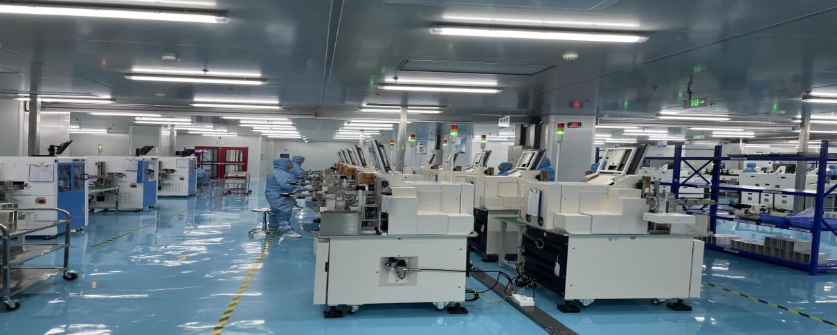
Based on the superior piezoelectric properties of epsilon(ε) phase gallium oxide thin film materials, the company has led the world in mass production of gallium oxide based surface/bulk acoustic wave RF filter chips with great quality. To this end, the company is building more than 50 production lines of ultra wide band-gap semiconductor RF chips and epitaxial wafer , focusing on 5G/6G communication, intelligent Internet of Things and precisely locating and other application fields. At that time, gallium oxide based acoustic RF filter chips RF power electronic chips and other globally competitive products will have generated an output value of more than 2 billion yuan. The company is committed to becoming a world leading compound semiconductor R&D, manufacturing and service company.
R&D Team
Professor Wang Gang of School of Microelectronics, Sun Yat sen University, is the chief scientist of the Sunwise team, and is recognized as an top expert in the field of photoelectronics in China. In March 2001, he obtained a doctorate degree in engineering from the National Nagoya University of Technology in Japan. During his doctorate period, he was mainly engaged in the research of MOCVD growth and the production technology of related photoelectronic devices. From April 2001 to April 2004, Professor Wang Gang worked in Fujitsu Quantum Components Company (Japan), mainly engaged in the research and development of 10Gp/s, 40Gp/s ultra-high speed optical communication devices.
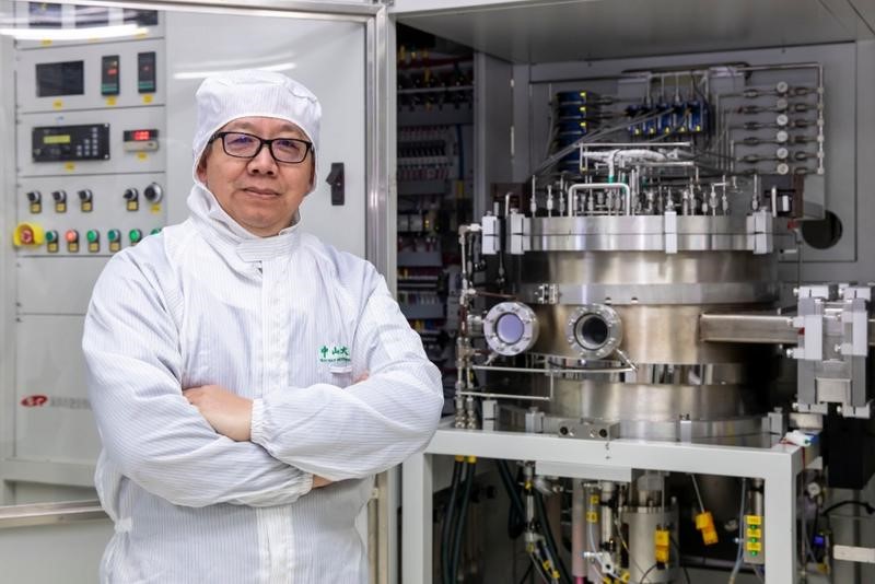
After returning to China in 2004, Professor Wang Gang successively served as a member of the general expert group of the "Eleventh Five Year Plan" and the "Twelfth Five Year Plan" National 863 Plan "Semiconductor Lighting Project" conducted by the Ministry of Science and Technology, and was selected as a New Century Talent by the Ministry of Education. Now he is the president of Foshan Research Institute of Sun Yat sen University. For a long time, he has been engaged in the research and development of wide band-gap oxide semiconductor thin film materials and devices, 3D printing and manufacturing technology development of 3D heterogeneous integrated chips for electronic devices, and he has been in high-end equipment research and development of semiconductor materials. In 2020, he won the second prize of "Guangdong Science and Technology Progress Award", and led his team to become a member of the "Science and Technology Innovation China Leading Technology List" in 2021.
Researcher Wang Mengyuan, who is in charge of Sunwise Semiconductor, has worked in the semiconductor industry for more than 20 years. He has been engaged in the research of the third generation semiconductor gallium nitride and ultra wide band-gap semiconductor materials, epitaxy and chip, and packaging process for a long time. He has technology and management experience of many years in semiconductor enterprise, and has carried out the development and international cooperation of many key common technologies, such as ZnO transparent conductive film chip technology, Ga2O3 wide band-gap piezoelectric film epitaxy growth technology, LED Thin GaN vertical structure chip manufacturing technology, and high color rendering index integrated light source module technology, and have made breakthrough achievements. As the first inventor, he has applied for more than 100 patents and is one of the inventors of the world's first ZnO chip and high color rendering index COB technology.

Achievements

the first 4-inch wafer with MOCVD-based ε- Ga2O3 thin film

MOCVD self-developed equipment

Heteroepitaxy on sapphire,silicon and silicon carbide substrates

Jingxu Team solves the key core issues of gallium oxide semiconductor material industrialization

wafer preparation includes substrate preparation and epitaxial process
