Paper Sharing
【International Papers】p-Type β-Ga₂O₃ Homoepitaxial Films with Superior Electrical Transport Properties
日期:2025-08-27阅读:654
Researchers from the Université Paris-Saclay have published a dissertation titled " p-Type β-Ga2O3 Homoepitaxial Films with Superior Electrical Transport Properties" in Advanced Photonics Research.
Background
To realize the full functionality of any emerging electronic technology based on UWBG semiconductors, both n- and p-type conductivity (i.e., bipolarity) should be attained. Till recently, a drawback with bipolar Ga2O3 technology was related to the absence of robust homoepitaxial p-type layers possessing high conductivity at room temperature. This obstacle has led to heterostructures mainly using polycrystalline p-NiO as p-type oxides. It is worth emphasizing that significant advancements have been made in the growth of high quality n-type homoepitaxial β-Ga2O3 thin-films on substrates with (–201), (100), (010), and (001) crystallographic orientations using MOCVD, MOVPE, LPCVD, HVPE, MBE. However, demonstrations of Ga2O3 homo p-n junctions are still handful. To efficiently address the urgent demand for p-n homojunction realization, the first necessary step is to grow high-quality p-type β-Ga2O3 layers with hole conductivity measurable at or near room temperature.
This work demonstrates high structural quality undoped p-type β-Ga2O3 epitaxial layers with distinct electrical transport properties grown on (–201)- and (010)-oriented gallium oxide substrates. Remarkable high hole concentration and mobility from 370 K for (010) β-Ga2O3 films opens a way for homojunction fabrication, simultaneously revealing the nature of electrical anisotropy related to crystallographic orientations. These findings are crucial for the realization of p-n homojunctions – essential building blocks for a wide range of power electronic and opto-electronic devices.
Abstract
This work reports high structural quality and exceptional electrical transport properties of homoepitaxial β-Ga2O3 thin films grown by Metal–Organic Chemical Vapor Deposition (MOCVD) on (010)- and (–201)-oriented substrates. (010) β-Ga2O3 samples exhibit mobility of up to 69.4 cm2 (V·s)−1 and stable hole concentrations ≈2.4 × 1017 cm−3 from 370 to 700 K. Structural and morphological studies, including XRD, AFM, and STEM, confirm high epitaxial quality, absence of extended defects and minimal strain. (–201) β-Ga2O3 layer, which is simultaneously grown, exhibits typical p-Ga2O3 behavior with observed deep level defects. The hole mobility ranging from 26 to 36 cm2 V−1·s−1 is measured between 420 and 700 K. Comparison of (010) and (–201) orientations reveals distinct anisotropic electrical properties. The findings emphasize the free motion of holes in β-Ga2O3 and the critical role of crystallographic orientation.
Conclusion
In this work, we demonstrated that β-Ga2O3 (010) and (–201) layers simultaneously grown by MOCVD exhibit p-type conductivity with pronounced anisotropic electrical transport properties, strongly dependent on the substrate's crystallographic orientation. Our measurements revealed that the (–201) layer has typical p-Ga2O3 behavior with deep level defects. At the same time, the hole mobility for this layer ranges from 26 to 36 cm2 V−1·s−1 for the temperatures between 420 and 700 K. The (010) layer, on the other hand, exhibited high free hole concentrations (2.4 × 1017 cm−3) at 370 K with high mobility of 69.4 cm2 V−1·s−1. High crystalline quality and the absence of extrinsic impurities and extended defects for the layers, grown on the substrates of both orientations, were confirmed by structural and compositional studies.

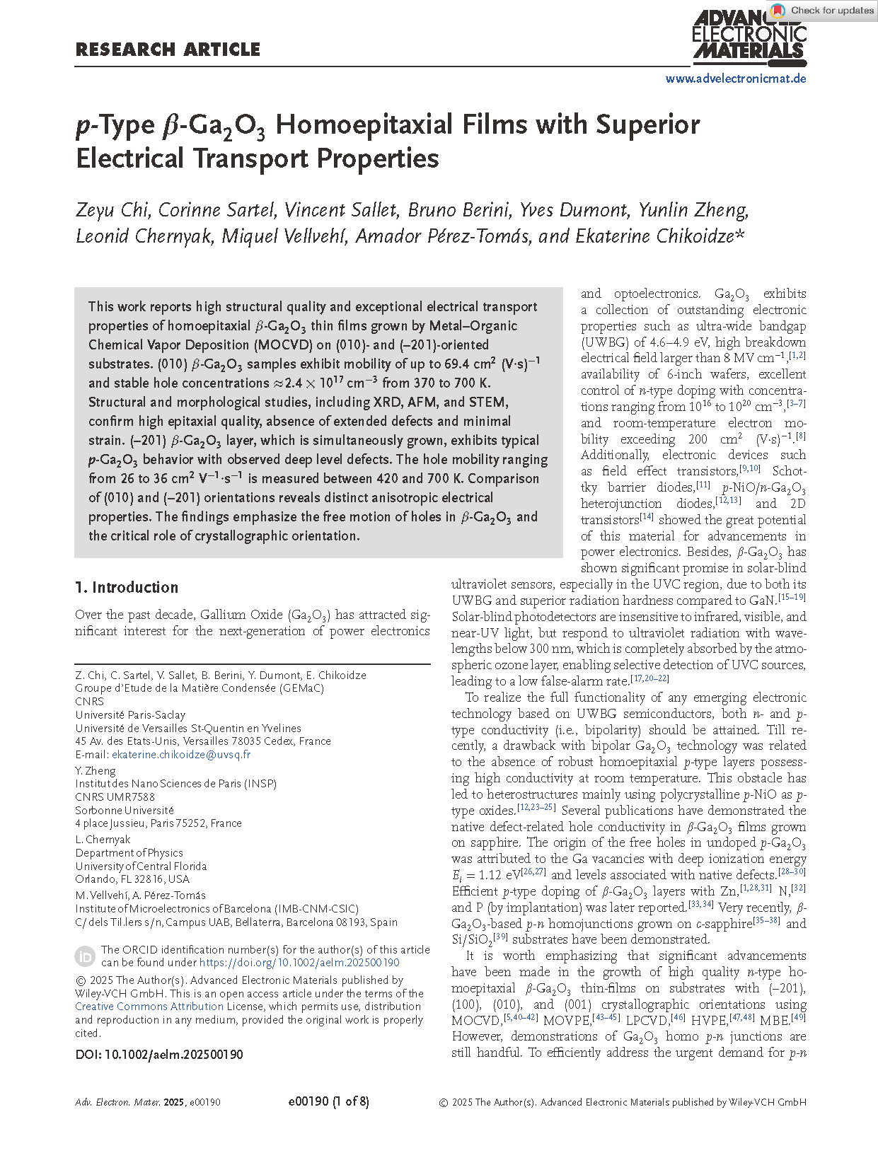
FIG.1 Electrical transport properties of homoepitaxially grown (–201) β-Ga2O3 sample: a) Temperature-dependent resistivity b) Hall voltage as a function of applied magnetic field at 500 K. c) Hall hole concentration and d) Hall hole mobilities versus temperature. Inset in (a) and (c): Arrhenius plots for conductivity and hole concentration, for the determination of activation energies for conductivity and carrier concentration, respectively.

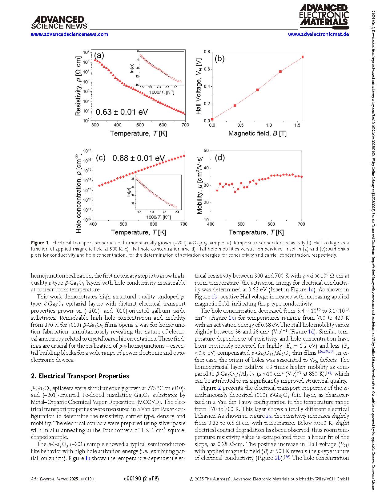
FIG 2. Electrical transport properties of homoepitaxially-grown β-Ga2O3 (010) sample: a) Temperature-dependent resistivity b) Hall voltage as a function of applied magnetic field at 500 K. c) Hall hole concentration and d) Hall hole mobilities versus temperature.

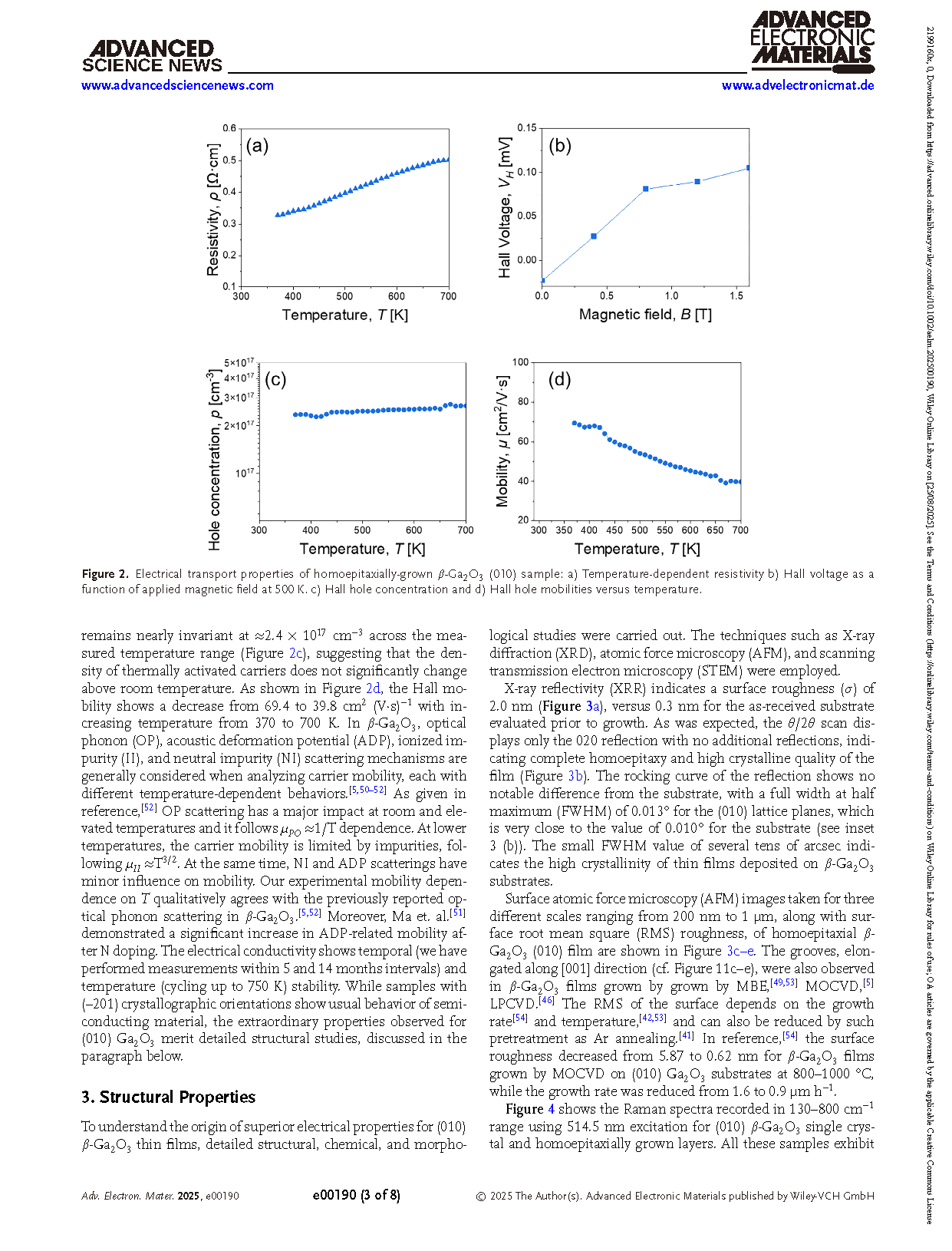
FIG.3 X-ray a) reflectivity and b) diffraction of homoepitaxial β-Ga2O3 (010) film (in red) compared with the scans of the substrates alone (in blue). σ in (a): surface roughness; inset in (b): rocking curves of 020 reflection where Δω is the deviation from the angle of incidence of θ/2θ. c–e): Surface AFM images taken for three different scales, with an overall RMS of 2.3 nm.

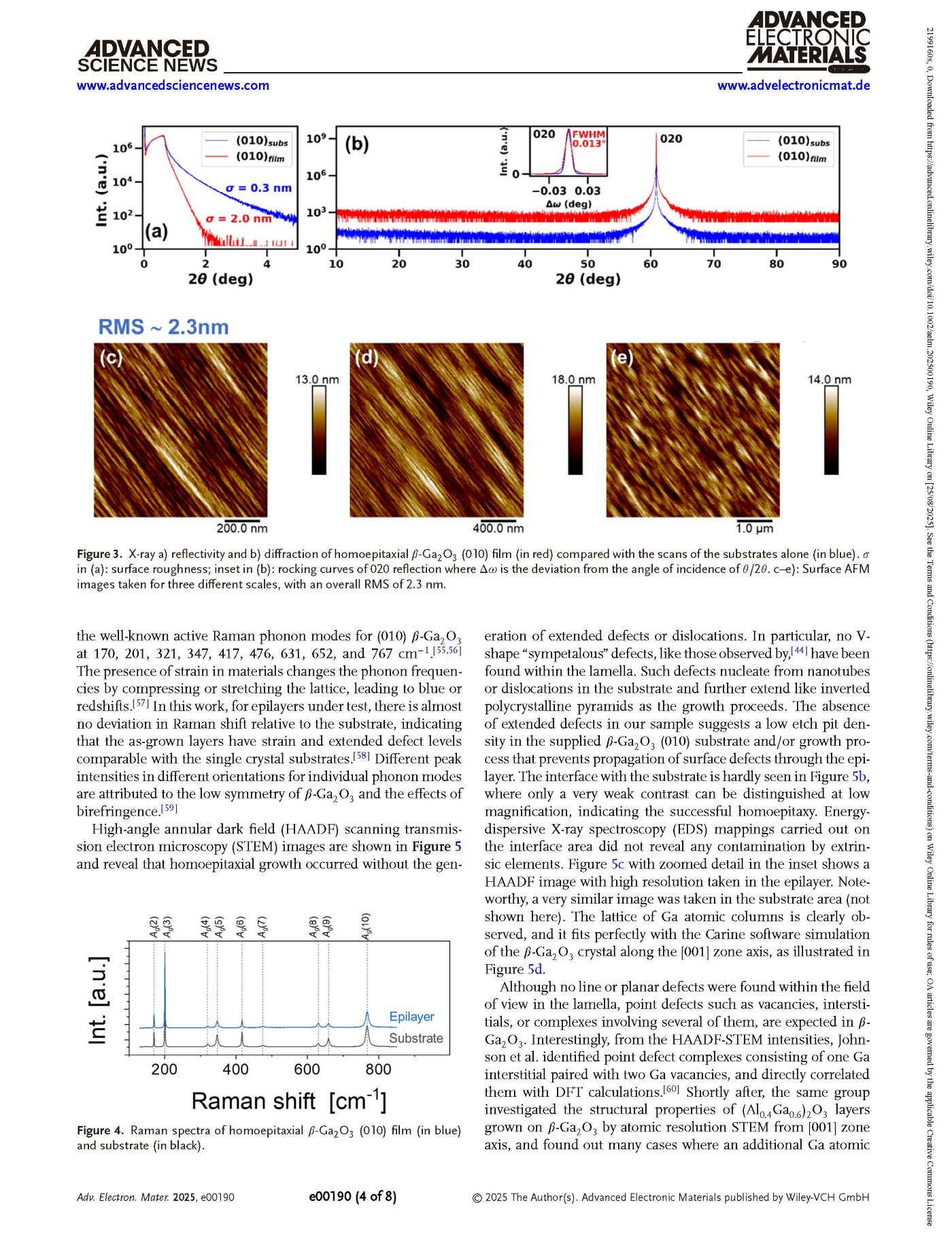
FIG.4 Raman spectra of homoepitaxial β-Ga2O3 (010) film (in blue) and substrate (in black).

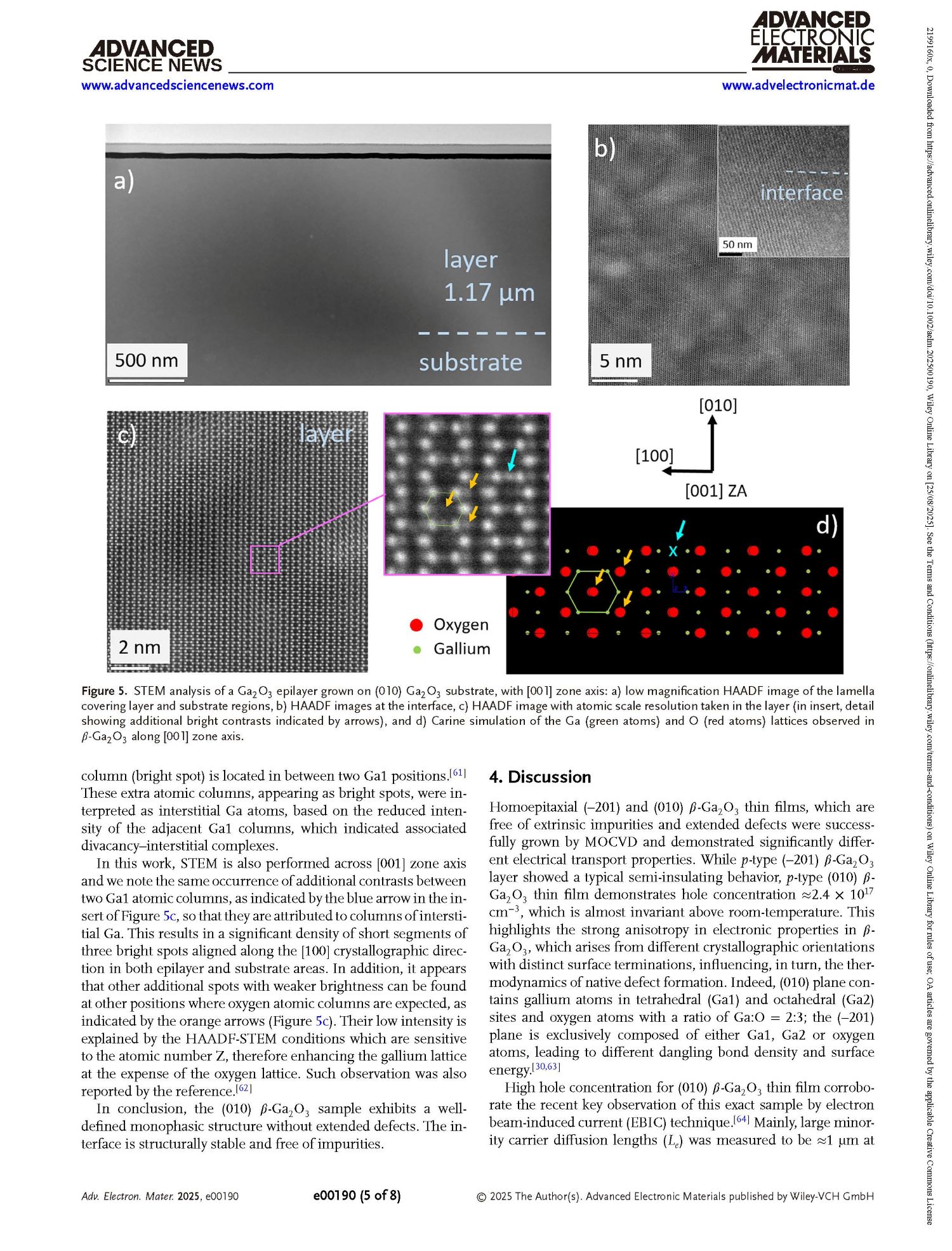
FIG.5 STEM analysis of a Ga2O3 epilayer grown on (010) Ga2O3 substrate, with [001] zone axis: a) low magnification HAADF image of the lamella covering layer and substrate regions, b) HAADF images at the interface, c) HAADF image with atomic scale resolution taken in the layer (in insert, detail showing additional bright contrasts indicated by arrows), and d) Carine simulation of the Ga (green atoms) and O (red atoms) lattices observed in β-Ga2O3 along [001] zone axis.
DOI:
doi.org/10.1002/aelm.202500190