Paper Sharing
【International Papers】Electron beam irradiation-induced transport and recombination in p-type gallium oxide grown on (001) β-Ga₂O₃ substrate
日期:2025-09-05阅读:617
Researchers from the University of Central Florida have published a dissertation titled "Electron beam irradiation-induced transport and recombination in p-type gallium oxide grown on (001) β-Ga2O3 substrate" in Journal of Applied Physics.
Abstract
This study investigates minority electron diffusion length and carrier recombination phenomena in p-type 300 nm-thick Ga2O3 films homoepitaxially grown over a (001) tin-doped β-Ga2O3 conductive substrate. This research is novel due to its systematic and near-simultaneous measurements in the top layer of a p-Ga2O3/n-Ga2O3 structure using independent electron beam-induced current and cathodoluminescence techniques. Previous work primarily focused on heteroepitaxial architectures or gallium oxide grown over insulating substrates of the same material. In this work, the activation energies related to point defects in gallium oxide were extracted from temperature-dependent incremental electron beam irradiation experiments to gain insight into the defect landscape and its influence on minority carrier transport and recombination dynamics.
Conclusion
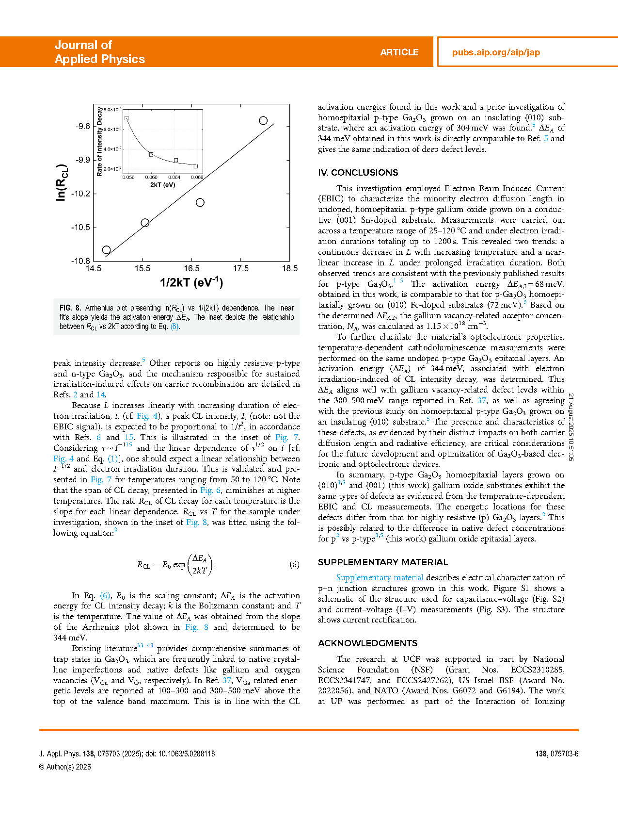
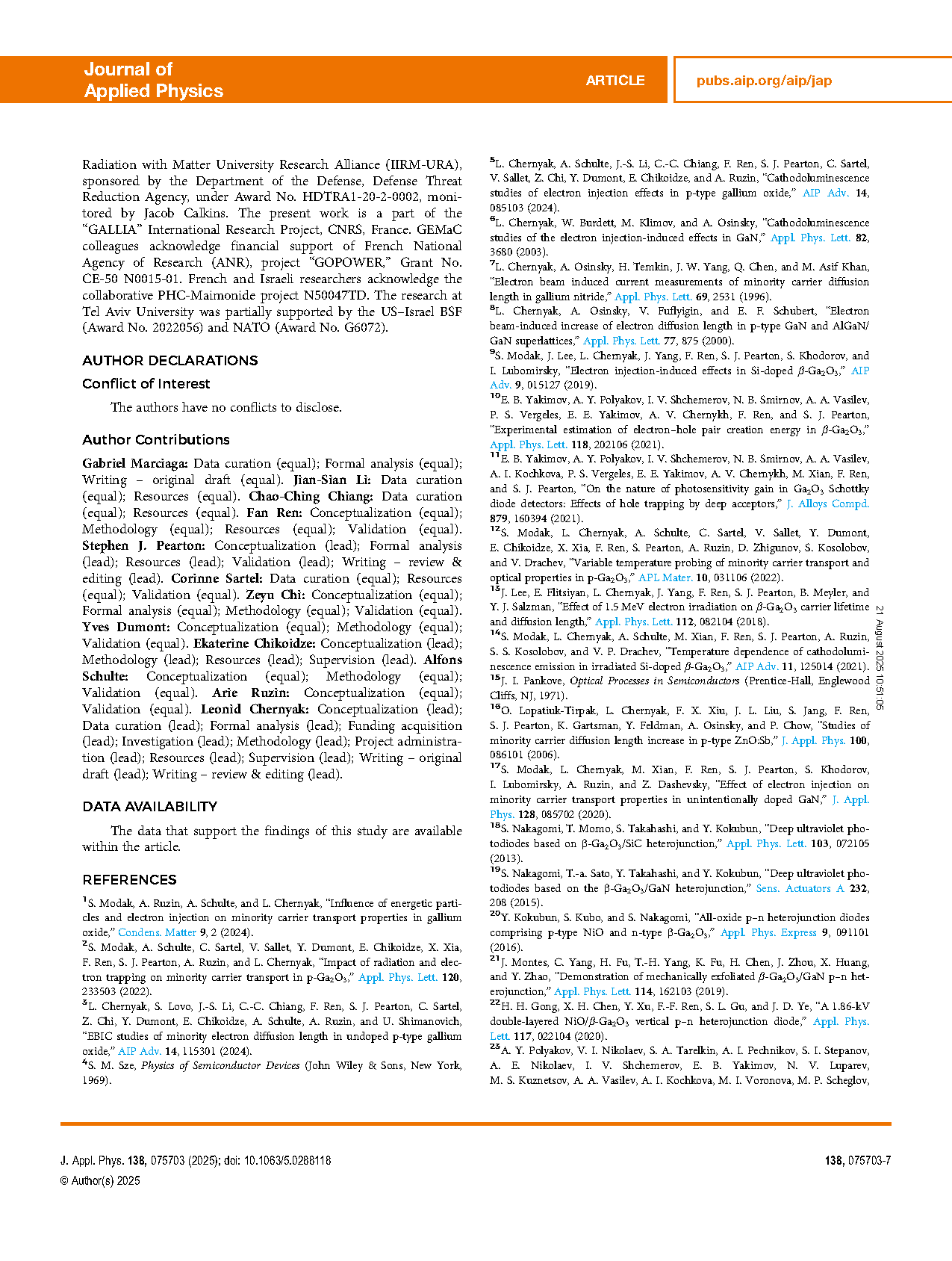
This investigation employed Electron Beam-Induced Current (EBIC) to characterize the minority electron diffusion length in undoped, homoepitaxial p-type gallium oxide grown on a conductive (001) Sn-doped substrate. Measurements were carried out across a temperature range of 25–120 °C and under electron irradiation durations totaling up to 1200 s. This revealed two trends: a continuous decrease in L with increasing temperature and a near-linear increase in L under prolonged irradiation duration. Both observed trends are consistent with the previously published results for p-type Ga2O3. The activation energy ΔEA,I = 68 meV, obtained in this work, is comparable to that for p-Ga2O3 homoepitaxially grown on (010) Fe-doped substrates (72 meV). Based on the determined ΔEA,I, the gallium vacancy-related acceptor concentration, NA, was calculated as 1.15 × 1018 cm−3.
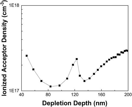
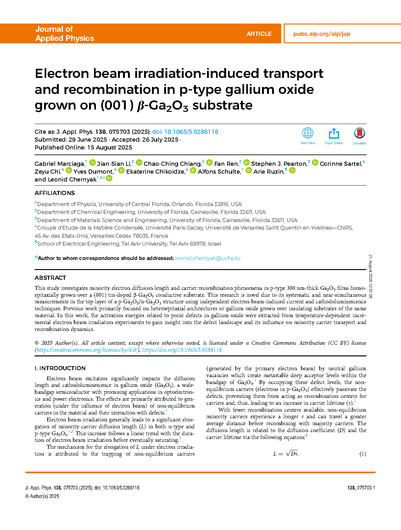
FIG.1 Ionized acceptor density measured at 450 K in the top p-type epilayer obtained between 40 and 200 nm of depth from the surface using capacitance–voltage (C–V) measurements.
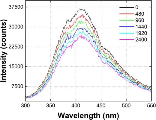
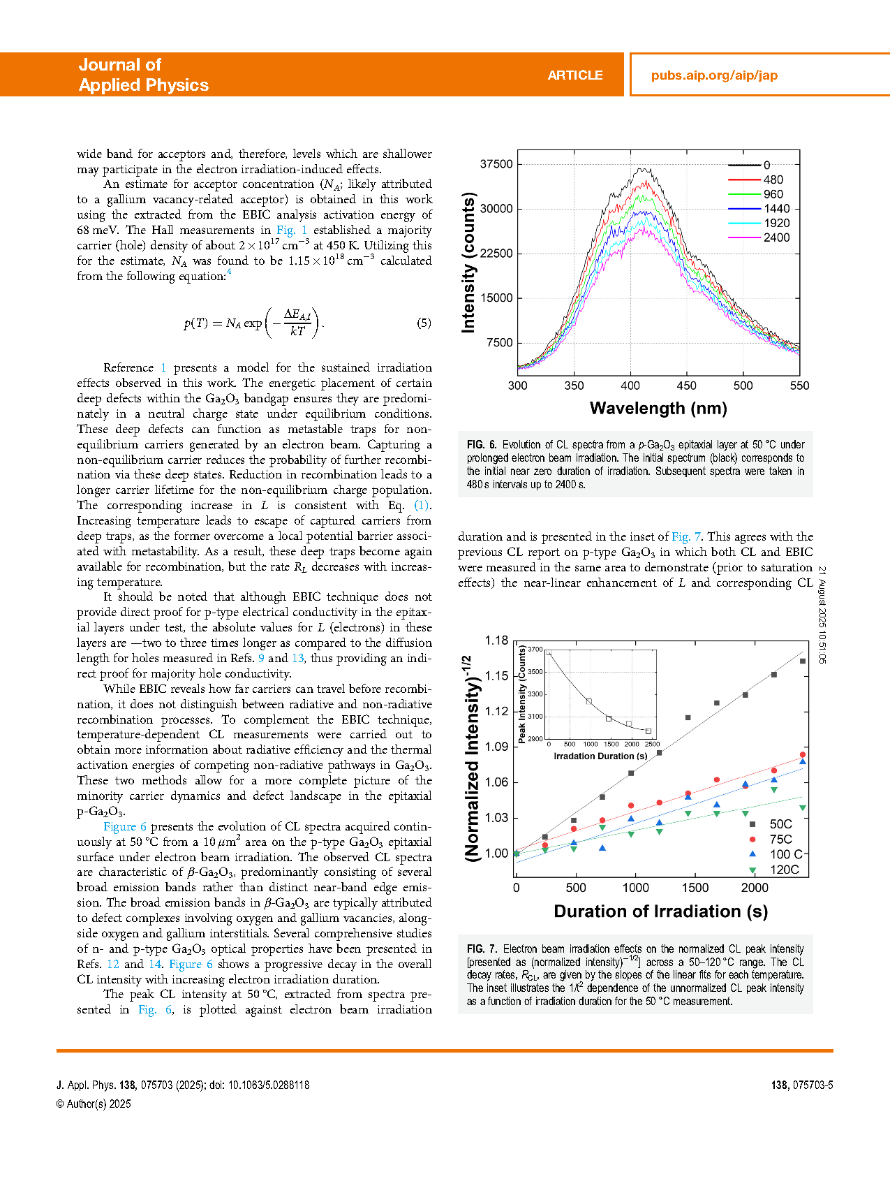
FIG.2 Evolution of CL spectra from a p-Ga2O3 epitaxial layer at 50 °C under prolonged electron beam irradiation. The initial spectrum (black) corresponds to the initial near zero duration of irradiation. Subsequent spectra were taken in 480 s intervals up to 2400 s.
DOI:
doi.org/10.1063/5.0288118