Paper Sharing
【Domestic Papers】Synergistic LPCVD and PECVD Growth of β-Ga₂O₃ Thin Films for High-Sensitivity and Low-Dose Direct X-Ray Detection
日期:2025-09-15阅读:624
Researchers from the Inner Mongolia University of Technology have published a dissertation titled " ynergistic LPCVD and PECVD Growth of β-Ga2O3 Thin Films for High-Sensitivity and Low-Dose Direct X-Ray Detection " in Nanomaterials.
Project Support
This research was funded by the Project of College Student Innovation and Entrepreneurship Training Program of China (No. S202410128015, Inner Mongolia Autonomous Region-level), the National Natural Science Foundation of China (Grant Nos. 12264035, 11864029, 62264013, and 62364014), the Natural Science Foundation of Inner Mongolia Autonomous Region of China (Grant No. 2024LHMS01013), and the Program for Young Talents of Science and Technology in Universities of Inner Mongolia Autonomous Region of China (Grant No. NJYT24065).
Background
In recent years, the wide bandgap semiconductor gallium oxide has emerged as a new material choice for exploring high-performance X-ray detectors due to its high density, excellent thermal and chemical stability, significant radiation resistance, and inherent rigid structure. Moreover, the X-ray absorption coefficient of Ga2O3 is far higher than that of diamond, comparable to that of Si and perovskite materials, and is less susceptible to visible light interference, which gives it significant advantages in the field of X-ray detection. Early work on unintentionally doped (UID) β-Ga2O3 single crystals established device feasibility for X-ray detection but suffered slow temporal response owing to abundant oxygen vacancies (VO). Fe doping increased resistivity and accelerated response through compensation of donor-like defects. Mg doping of a single crystal β-Ga2O3 simultaneously raised resistivity, suppressed VO, and delivered 16 times the sensitivity of a-Se. Al alloying widened the bandgap of single-crystal β-Ga2O3, lowering intrinsic carrier density and enabling high sensitivity. Thus, intentional dopants (Fe, Mg, Al) systematically couple defect suppression with resistivity/band engineering to enhance performance. Although X-ray detectors based on Ga2O3 single crystals have made significant progress, there are still certain challenges in the integration of functional modules and large-scale applications due to difficulties in growing large-sized, high-quality single crystals and the lack of effective P-type doping.
Abstract
Ultra-wide bandgap β-Ga2O3 is a promising low-cost alternative to conventional direct X-ray detector materials that are limited by fabrication complexity, instability, or slow temporal response. Here, we comparatively investigate β-Ga2O3 thin films grown on c-sapphire by low-pressure chemical vapor deposition (LPCVD) and plasma-enhanced CVD (PECVD), establishing a quantitative linkage between growth kinetics, microstructure, defect landscape, and X-ray detection figures of merit. The LPCVD-grown film (thickness ≈ 0.289 μm) exhibits layered coalesced grains, a narrower rocking curve (FWHM = 1.840°), and deep-level oxygen-vacancy-assisted high photoconductive gain, yielding a high sensitivity of 1.02 × 10⁵ μC Gyair−1 cm−2 at 20 V and a thickness-normalized sensitivity of 3.539 × 10⁵ μCGyair−1 cm−2 μm−1. In contrast, the PECVD-grown film (≈1.57 μm) shows dense columnar growth, higher O/Ga stoichiometric proximity, and shallow-trap dominance, enabling a lower dark current, superior dose detection limit (30.13 vs. 57.07 nGyair s−1), faster recovery, and monotonic SNR improvement with bias. XPS and dual exponential transient analysis corroborate a deep-trap persistent photoconductivity mechanism in LPCVD versus moderated shallow trapping in PECVD. The resulting high-gain vs. low-noise complementary paradigm clarifies defect–gain trade spaces and provides a route to engineer β-Ga2O3 thin-film X-ray detectors that simultaneously target high sensitivity, low dose limit, and temporal stability through trap and electric field management.
Conclusions
In summary, β-Ga2O3 thin films were grown on c-plane sapphire by using LPCVD and PECVD techniques, and MSM-type X-ray detectors were fabricated. It is demonstrated that the films grown by LPCVD were thin (289 nm), where slower surface kinetics favor lateral grain coalescence and reduced mosaic tilt (narrower rocking curve), while PECVD plasma activation induces rapid multi-site nucleation and columnar advancement, increasing tilt dispersion yet improving thickness scalability and film densification.
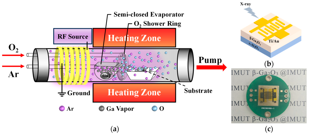
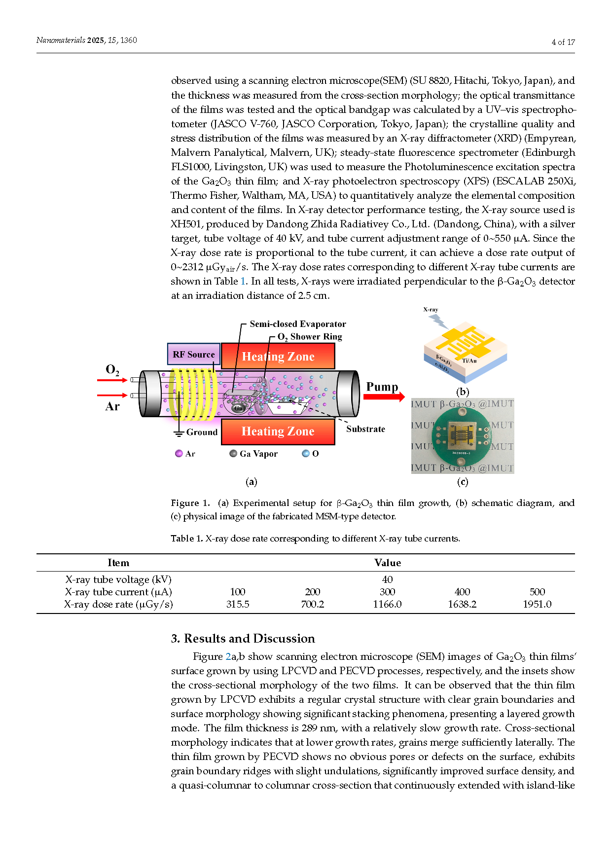
Figure 1. (a) Experimental setup for β-Ga2O3 thin film growth, (b) schematic diagram, and (c) physical image of the fabricated MSM-type detector.
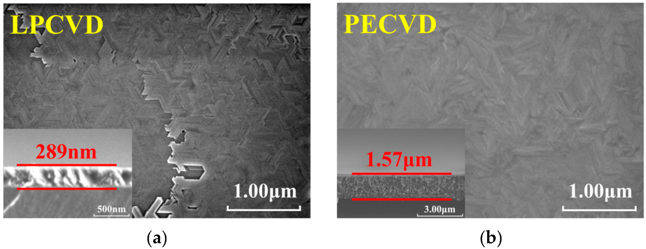
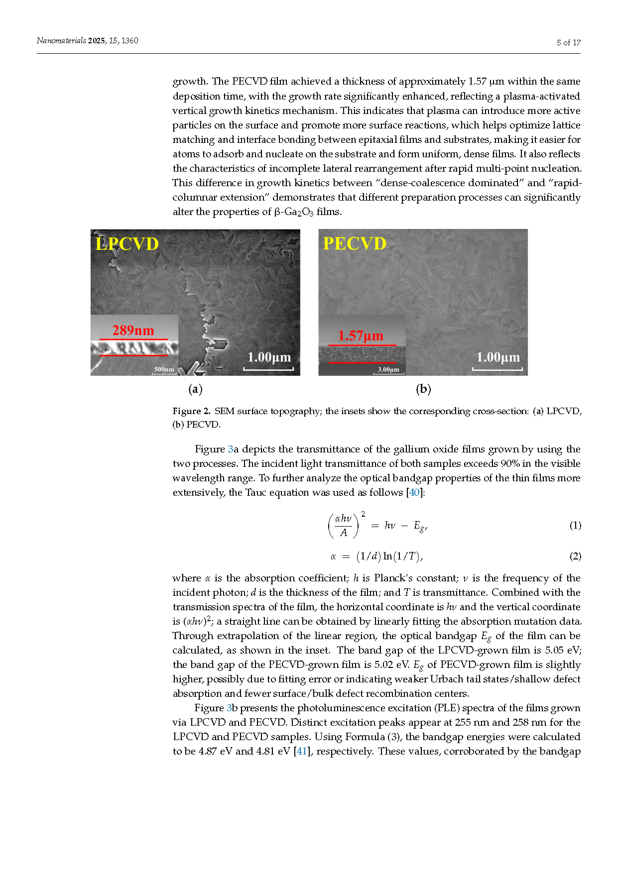
Figure 2. SEM surface topography; the insets show the corresponding cross-section: (a) LPCVD, (b) PECVD.
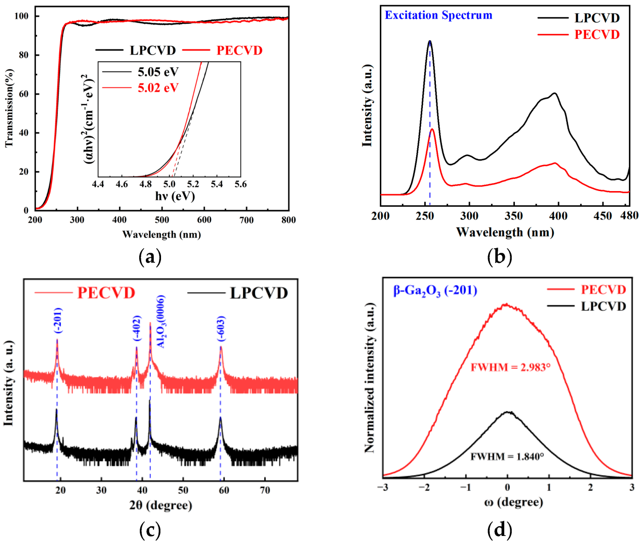
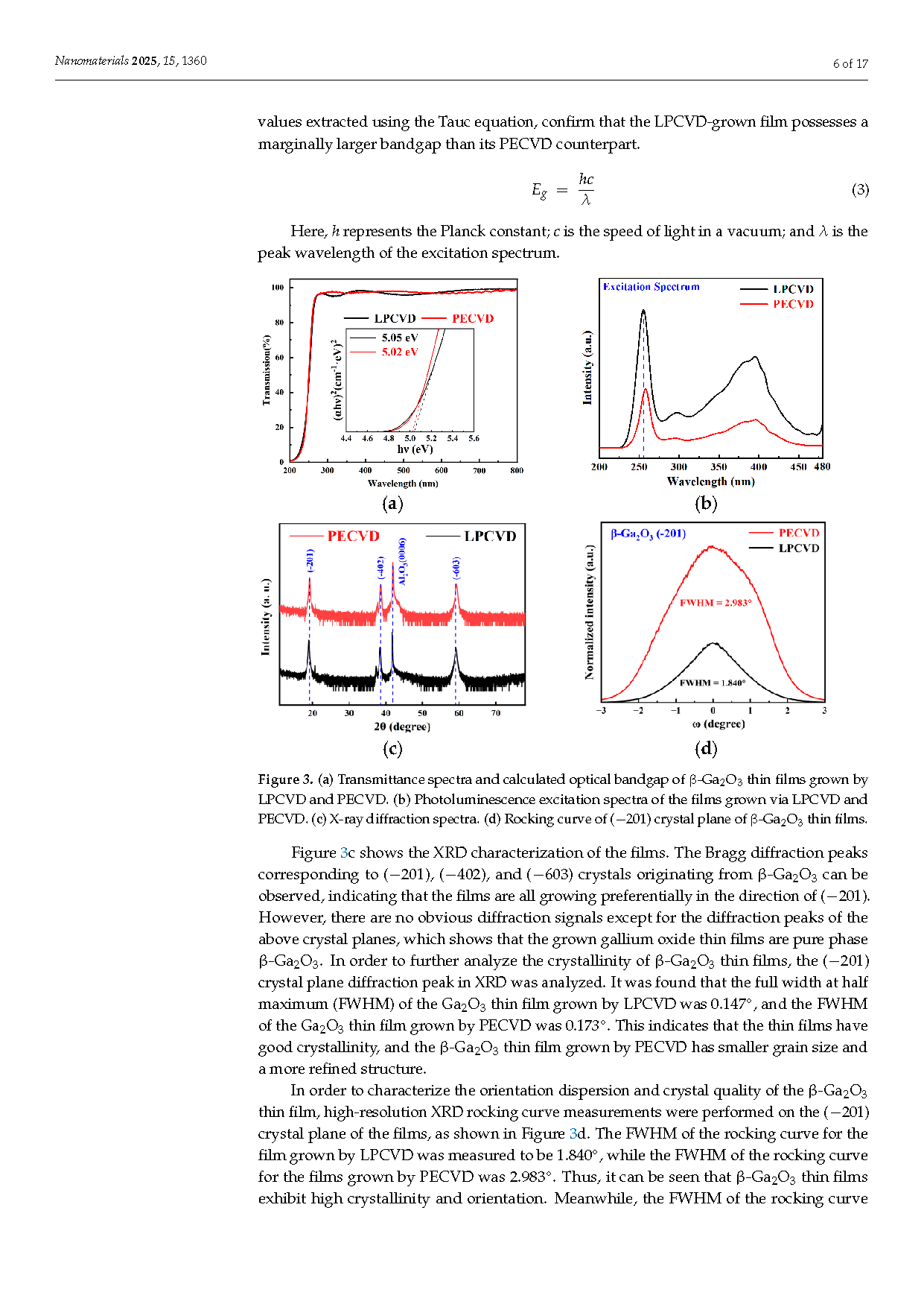
Figure 3. (a) Transmittance spectra and calculated optical bandgap of β-Ga2O3 thin films grown by LPCVD and PECVD. (b) Photoluminescence excitation spectra of the films grown via LPCVD and PECVD. (c) X-ray diffraction spectra. (d) Rocking curve of (−201) crystal plane of β-Ga2O3 thin films.
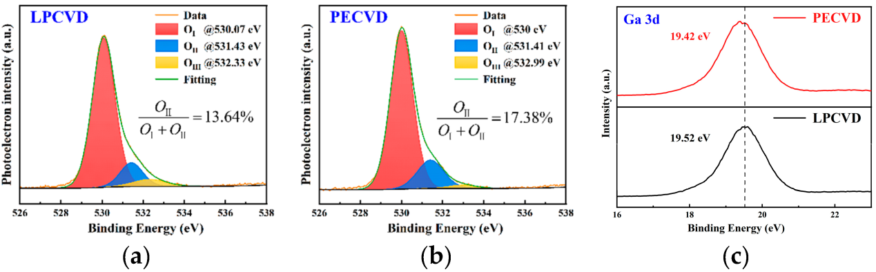
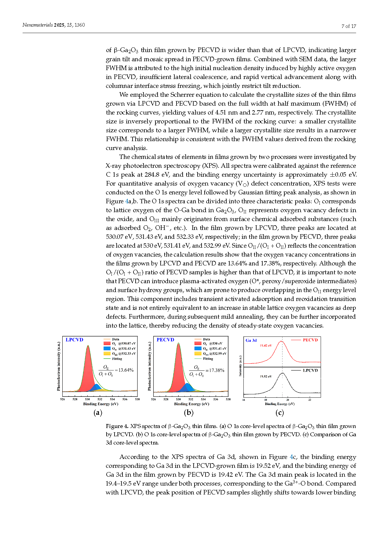
Figure 4. XPS spectra of β-Ga2O3 thin films. (a) O 1s core-level spectra of β-Ga2O3 thin film grown by LPCVD. (b) O 1s core-level spectra of β-Ga2O3 thin film grown by PECVD. (c) Comparison of Ga 3d core-level spectra.
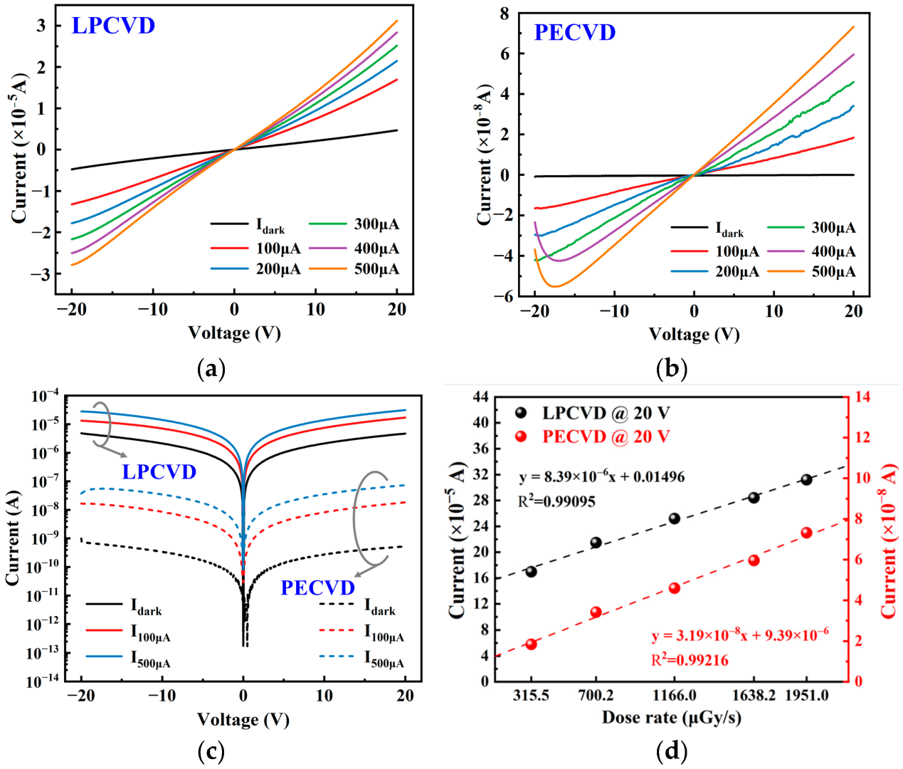
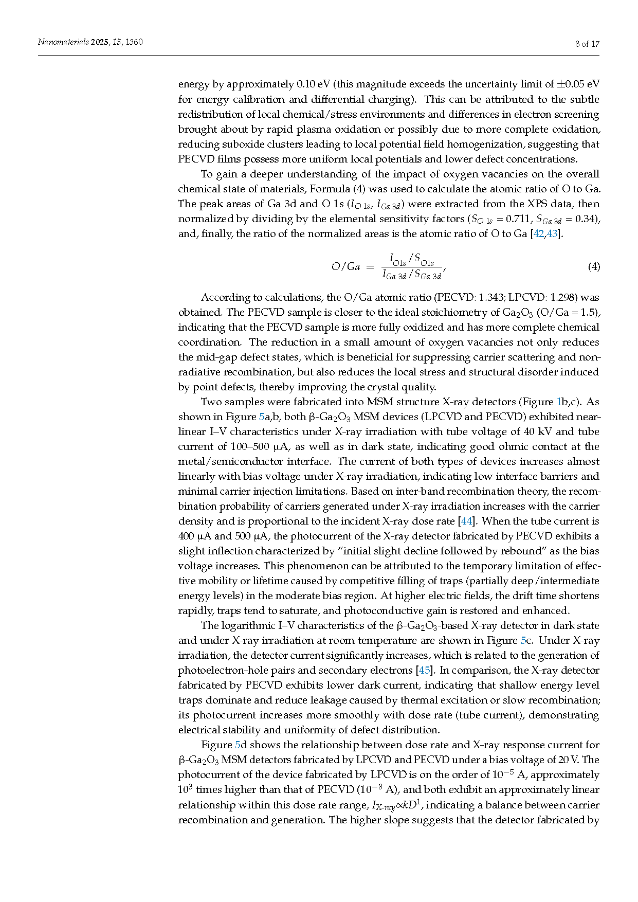
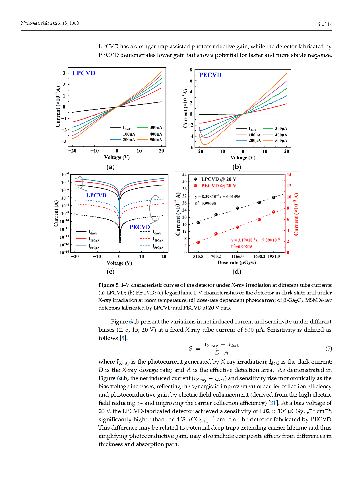
Figure 5. I–V characteristic curves of the detector under X-ray irradiation at different tube currents: (a) LPCVD; (b) PECVD; (c) logarithmic I–V characteristics of the detector in dark state and under X-ray irradiation at room temperature; (d) dose-rate dependent photocurrent of β-Ga2O3 MSM X-ray detectors fabricated by LPCVD and PECVD at 20 V bias.
DOI:
doi.org/10.3390/nano15171360