Paper Sharing
【International Papers】Unipolar β-Ga₂O₃ Pseudo-junction barrier Schottky diodes via Low-Cost magnesium diffusion process
日期:2025-09-15阅读:619
Researchers from the KAUST have published a dissertation titled "Unipolar β-Ga2O3 Pseudo-junction barrier Schottky diodes via Low-Cost magnesium diffusion process" in APL Materials.
Background
Ultra-wide bandgap (UWBG) semiconductors have attracted significant attention as key materials for next-generation power electronics. Among these, beta-gallium oxide (β-Ga2O3) stands out due to its ultra-wide bandgap of ~4.8 eV, high breakdown field (~8 MV/cm), and cost-effective bulk substrate growth, making it a promising candidate for high-voltage power devices. Diodes are fundamental in power circuits, and Junction Barrier Schottky (JBS) diodes combine low turn-on voltage with enhanced breakdown voltage through p-type grids near the Schottky interface. However, the lack of reliable p-type β-Ga2O3 has driven exploration of alternatives such as p-type NiOx, which faces issues including lower bandgap, lattice mismatch, and interface recombination. Recently, magnesium (Mg) diffusion has emerged as a method to create high-resistance electron-blocking layers, demonstrated in both GaN andβ-Ga2O3 devices. Existing approaches like Mg-doped Spin-on-Glass or high-temperature (>1000 °C) diffusion are complex and costly. This work proposes a low-cost, room-temperature compatible Mg diffusion technique directly into selected regions of β-Ga2O3 substrates to form high-resistance areas, enabling Schottky barrier diode (SBD) devices with enhanced breakdown voltage, reduced processing temperature, and simplified fabrication, providing a practical route for β-Ga2O3 JBS device development.
Abstract
Beta Gallium Oxide (Ga2O3) Junction Barrier Schottky diodes possess excellent breakdown characteristics and efficiency, but the lack of p-type Ga2O3 has led to the use of alternative materials, such as NiOx, which pose challenges regarding lattice mismatch and temperature stability. This work reports a unipolar Ga2O3 diode enabled by the magnesium (Mg) diffusion process to create high-resistance electron-blocking regions. The Mg diffusion process developed in this work uses a room temperature compatible chemical process followed by an 800 °C annealing step, which is lower compared to already reported methods in the literature. Therefore, the proposed method is thought to reduce the device processing temperature budget and hence cost. The resulting device achieves an Ion/Ioff ratio of ∼109, a knee voltage of ∼0.9 V, and a breakdown voltage of 596 V. In addition, it demonstrates stable operation from 100 to 500 K, highlighting its suitability for electronics operating across a broad temperature range.
Conclusion
This work demonstrates a β-Ga2O3 SBD enabled by Mg diffusion into selected areas of the β-Ga2O3 substrate to create highly resistive regions. The proposed methodology offers a low-cost, silicon-free solution optimized for Mg diffusion. The fabricated SBD having Mg diffusion regions outperformed the regular SBD; the proposed diode offered a significant improvement in breakdown voltage without introducing any serious compromise in the ON-state characteristics. Finally, the proposed diode is shown to offer suitable performance over a wide range of temperature, making it a promising device for extreme harsh electronics.
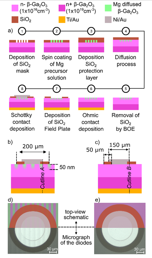
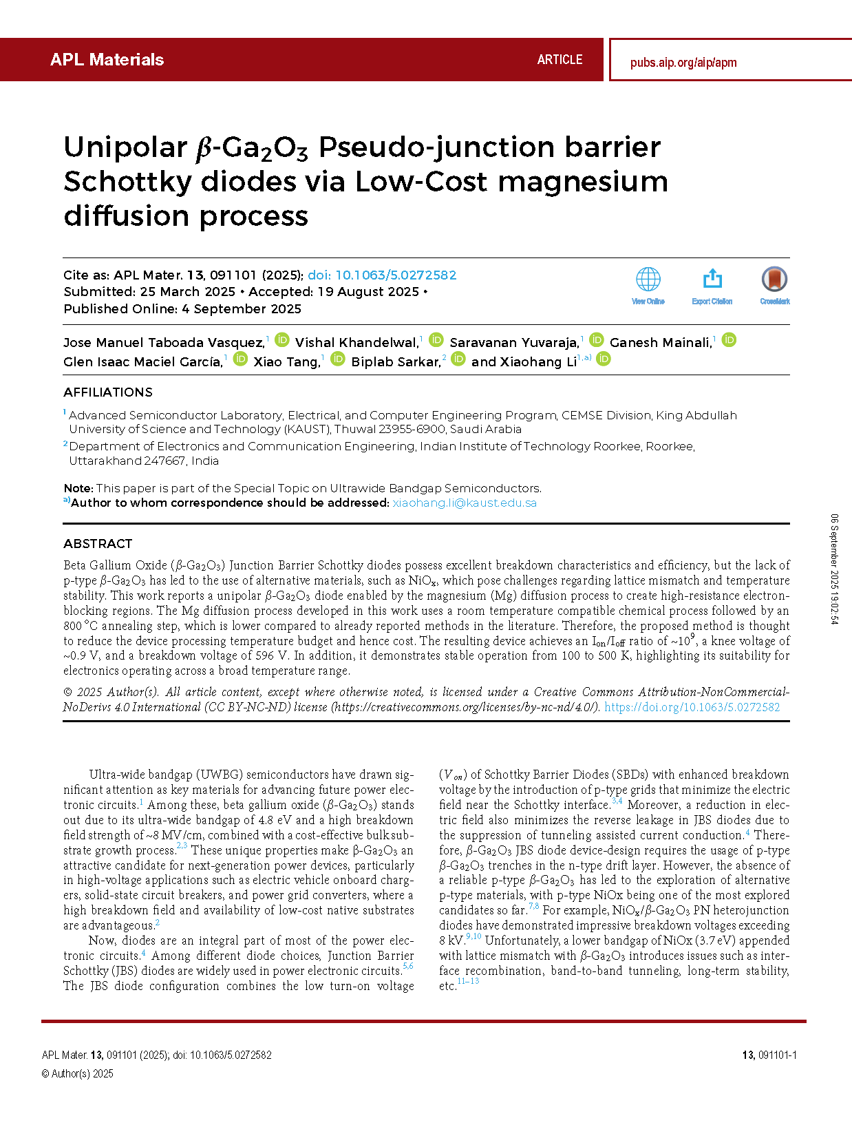
FIG.1 (a) Graphical illustration of the fabrication process developed to realize the proposed β-Ga2O3 SBD having Mg diffused regions; (b) and (c) cross-sectional schematic of SBD-1 and SBD-2, respectively; (d) and (e) top view schematic and micrograph of the fabricated SBD-1 and SBD-2, respectively.
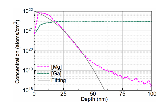
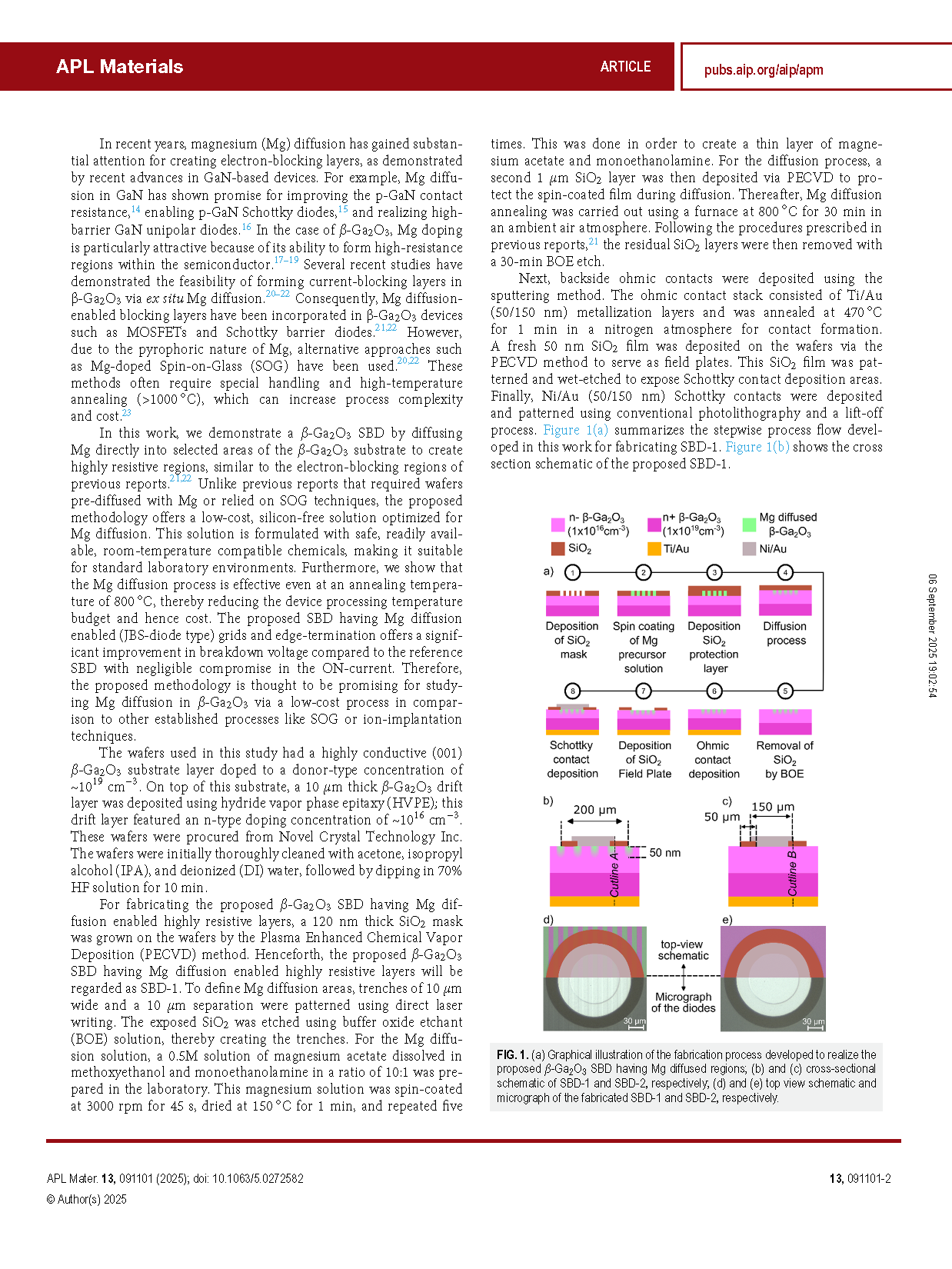
FIG.2 SIMS measured the profile highlighting the Mg concentration inside the β-Ga2O3 film.
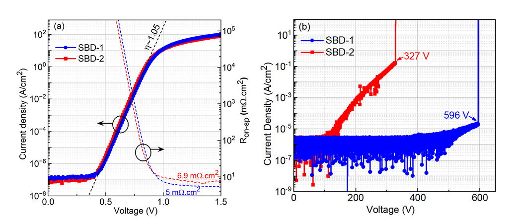
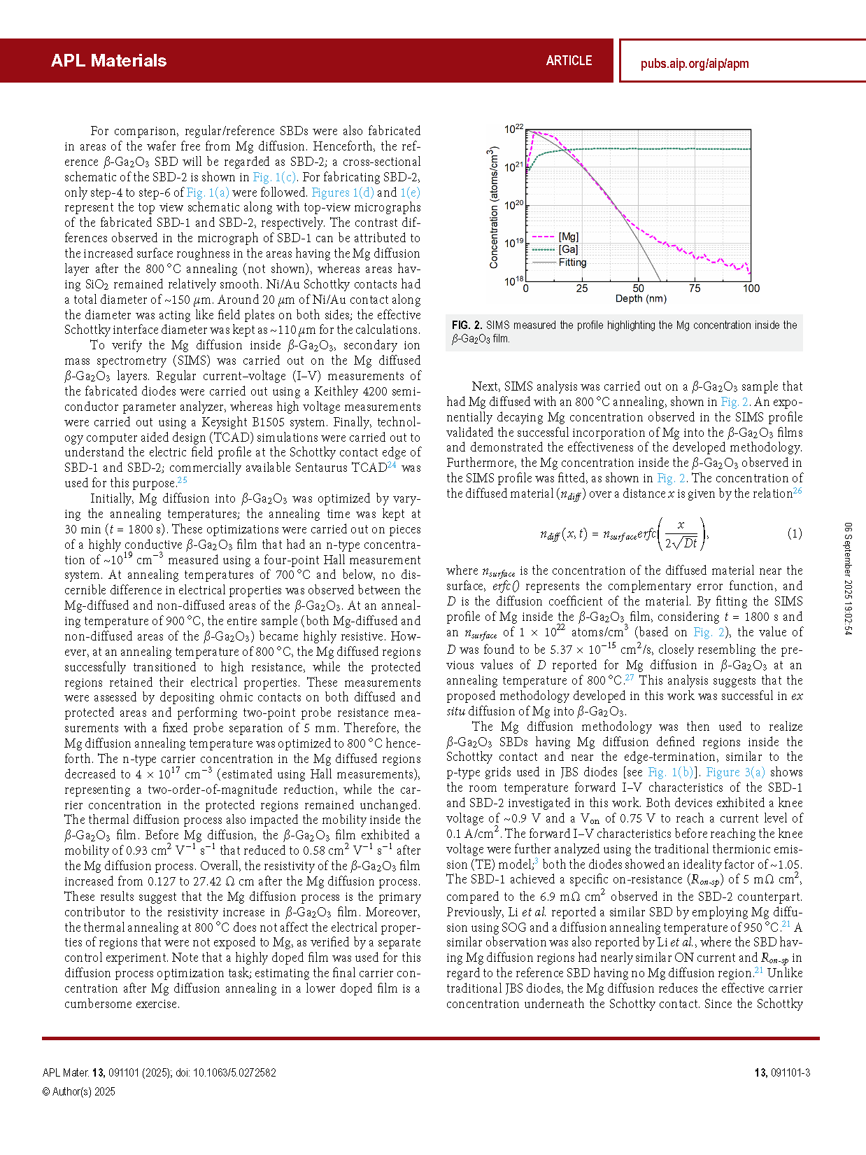
FIG.3 (a) Forward bias and (b) reverse breakdown characteristics of SBD-1 and SBD-2 investigated in this work.
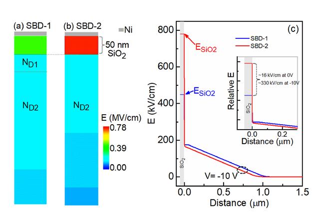
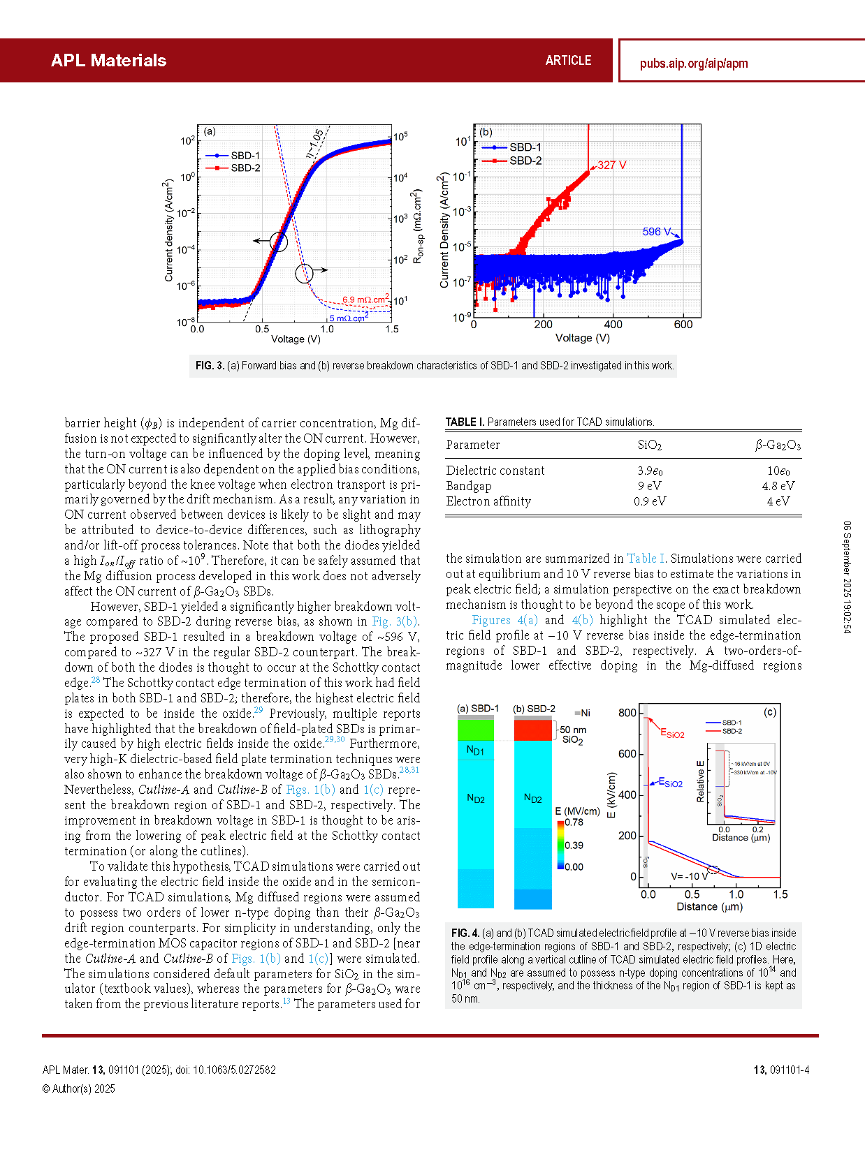
FIG.4 (a) and (b) TCAD simulated electric field profile at −10 V reverse bias inside the edge-termination regions of SBD-1 and SBD-2, respectively; (c) 1D electric field profile along a vertical cutline of TCAD simulated electric field profiles. Here, ND1 and ND2 are assumed to possess n-type doping concentrations of 1014 and 1016 cm−3, respectively, and the thickness of the ND1 region of SBD-1 is kept as 50 nm.
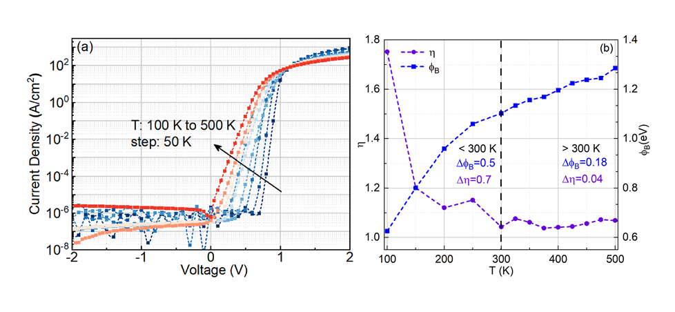
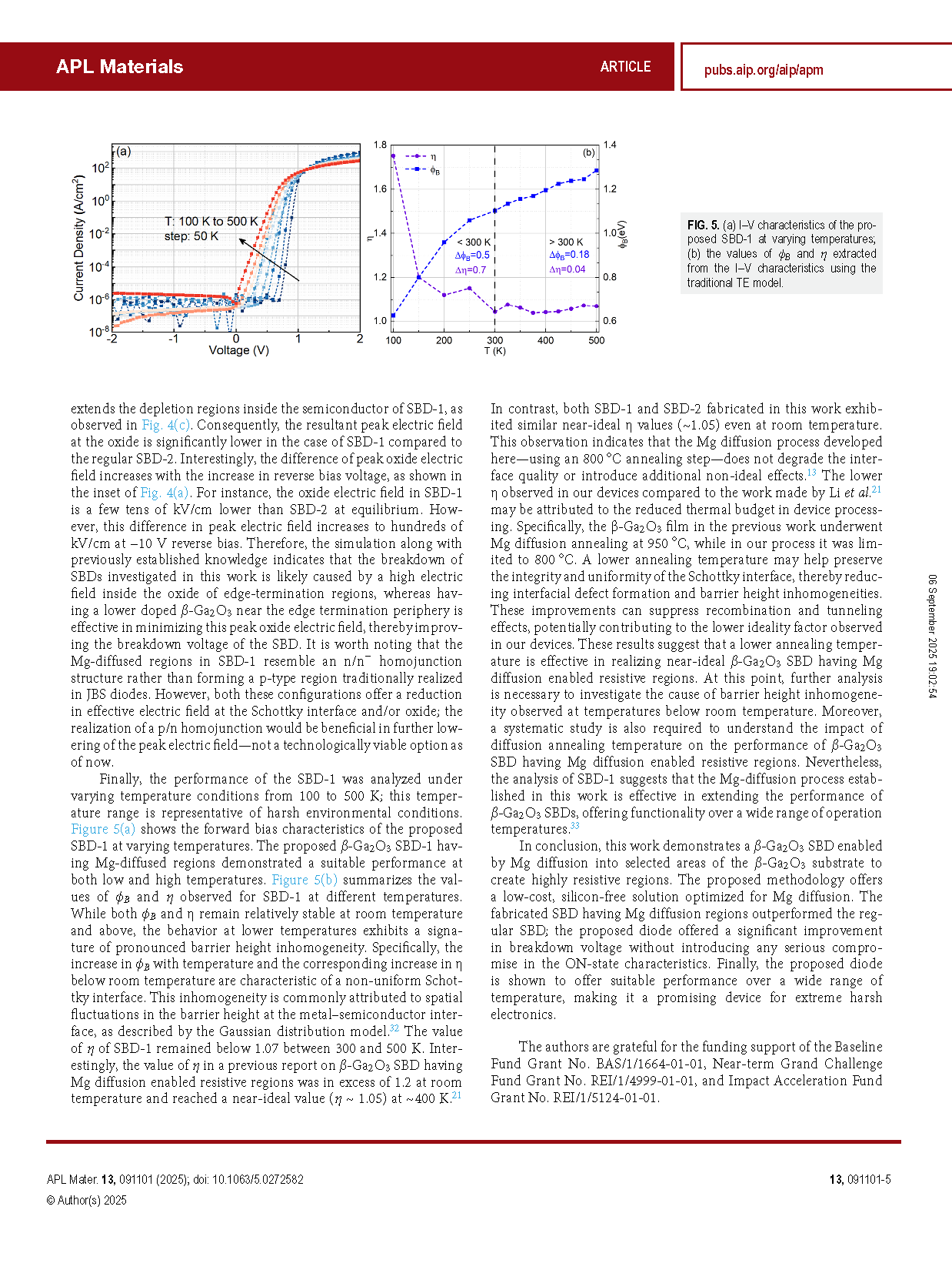
FIG.5 (a) I–V characteristics of the proposed SBD-1 at varying temperatures; (b) the values of ΦB and η extracted from the I–V characteristics using the traditional TE model.
DOI:
doi.org/10.1063/5.0272582