Paper Sharing
【International Papers】Structural and Electrically Conductive Properties of Plasma-Enhanced Chemical-Vapor-Deposited High-Resistivity Zn-Doped β-Ga₂O₃ Thin Films
日期:2025-09-16阅读:565
Researchers from the Lobachevsky State University have published a dissertation titled "Structural and Electrically Conductive Properties of Plasma-Enhanced Chemical-Vapor-Deposited High-Resistivity Zn-Doped β-Ga2O3 Thin Films" in Micromachines.
Background
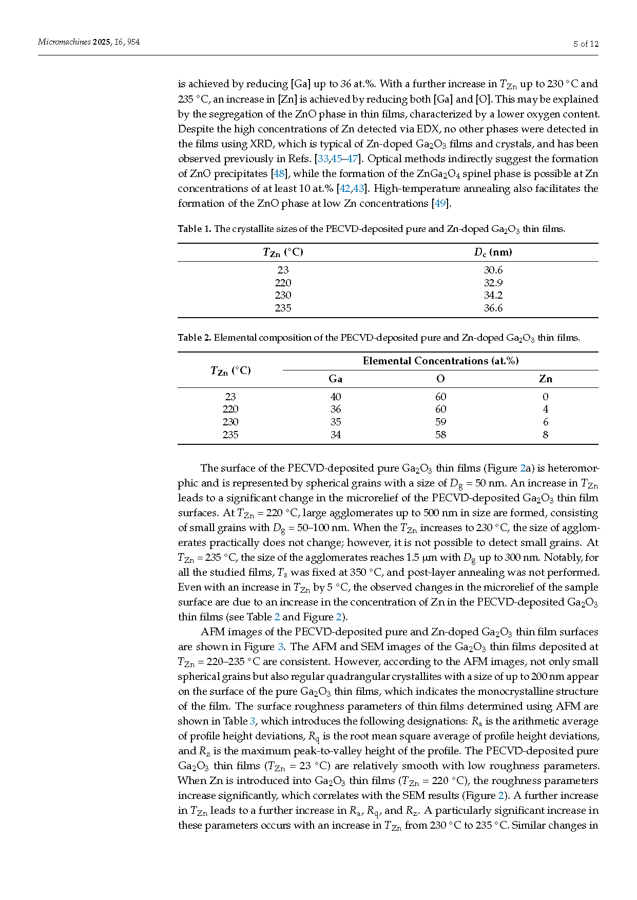
Despite theoretical predictions, it was not possible to obtain p-type conductivity by doping Ga2O3 with Zn in practice. It was later shown that Zn acts as a deep acceptor, compensating for the small donor levels of defects formed during material growth, which leads to an increase in Ga2O3 resistivity. It is thus possible to create layers with high and low conductivity in the Ga–Zn–O system using PECVD with the same precursors and tooling. This work focuses on the deposition and investigation of the structural and electrically conductive properties of Ga2O3 films doped with Zn and deposited via PECVD with pre-purification of the precursors. This is the first time that Ga2O3:Zn films have been deposited via PECVD with pre-purification of Ga and Zn precursors, with the advantages of this technique presented above. PECVD and its various modifications have proven to be scalable, highly reproducible, and easy to automate and implement, leading to their widespread industrial use for deposition of thin semiconductor films for various applications.
Abstract
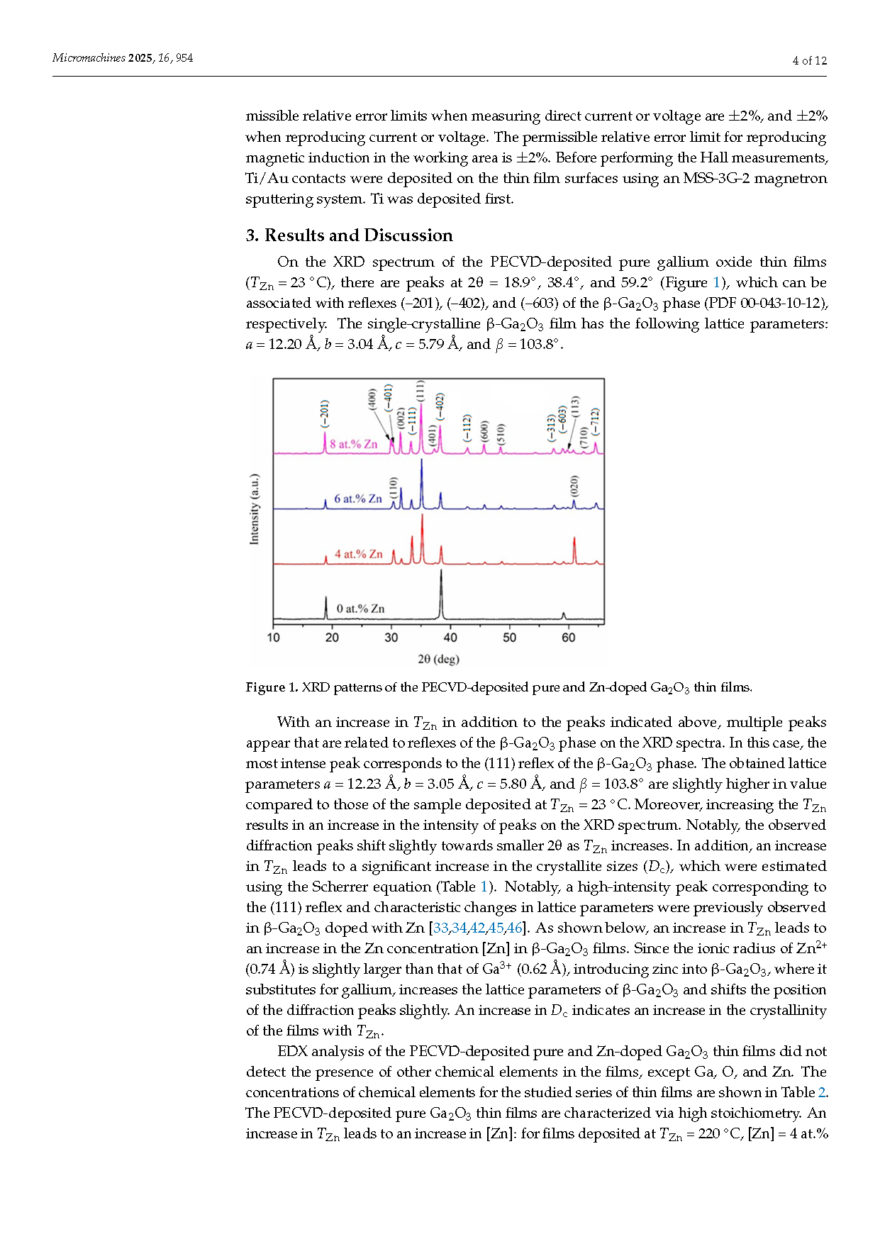
A method was developed for plasma-enhanced chemical vapor deposition of β-Ga2O3:Zn thin films with the possibility of pre-purifying precursors. The structural and electrically conductive properties of β-Ga2O3:Zn thin films were studied. Increasing the temperature of the Zn source (TZn) to 220 °C led to the formation of Ga2O3 films with a Zn concentration of 4 at.%, at TZn = 230 °C [Zn] = 6 at.% and at 235 °C. [Zn] = 8 at.% At TZn = 23 °C, the films corresponded to the β-Ga2O3 phase and were single-crystalline with a surface orientation of (–201). As TZn increased, the polycrystalline structure of β-Ga2O3 films with a predominant orientation of (111) was formed. The introduction of Zn led to the formation of a more developed microrelief of the surface. Raman spectroscopy showed that a small concentration of impurity atoms tended to replace gallium atoms in the oxide lattice, which was also confirmed by the Hall measurements. The concentration of charge carriers upon the introduction of Zn, which is a deep acceptor, decreased by 2–3 orders of magnitude, which mainly determined the decrease in the films’ resistivity. The resulting thin films were promising for the development of high-resistivity areas of β-Ga2O3-based devices.
Conclusions
A method was developed for plasma-enhanced chemical vapor deposition of β-Ga2O3:Zn thin films with the possibility of pre-purifying metal precursors. Increasing the temperature of the Zn source (TZn) to 220 °C led to the formation of Ga2O3 thin films with an impurity concentration of 4 at.%, at TZn = 230 °C [Zn] = 6 at.% and at 235 °C [Zn] = 8 at.%. The phase composition of the films, regardless of TZn, corresponded to the monoclinic β-Ga2O3 phase. At TZn = 23 °C, the β-Ga2O3 films were single-crystalline with a surface orientation of (–201). As TZn increased, a polycrystalline structure of β-Ga2O3 films with a predominant orientation of (111) was formed. Doping films with Zn led to a slight increase in the lattice parameters of the crystal and a significant increase in the size of the crystallites. The introduction of Zn also led to the formation of a more developed microrelief of the film surface, an increase in roughness parameters by about two orders of magnitude and in grain size by up to 300 nm, and the formation of grain agglomerates with a size of up to 1.5 µm. Raman spectroscopy showed that a small concentration of impurity atoms tended to replace gallium atoms in the oxide lattice, which was also confirmed by the results of the Hall measurements. The concentration of charge carriers upon the introduction of Zn, which is a deep acceptor, decreased by 2–3 orders of magnitude, which mainly determined the decrease in film resistivity. The mobility of charge carriers was determined to a greater extent by the microstructure of the films and weakly depended on [Zn].
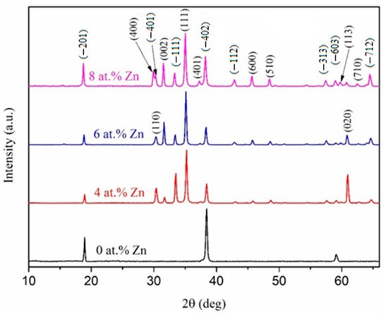
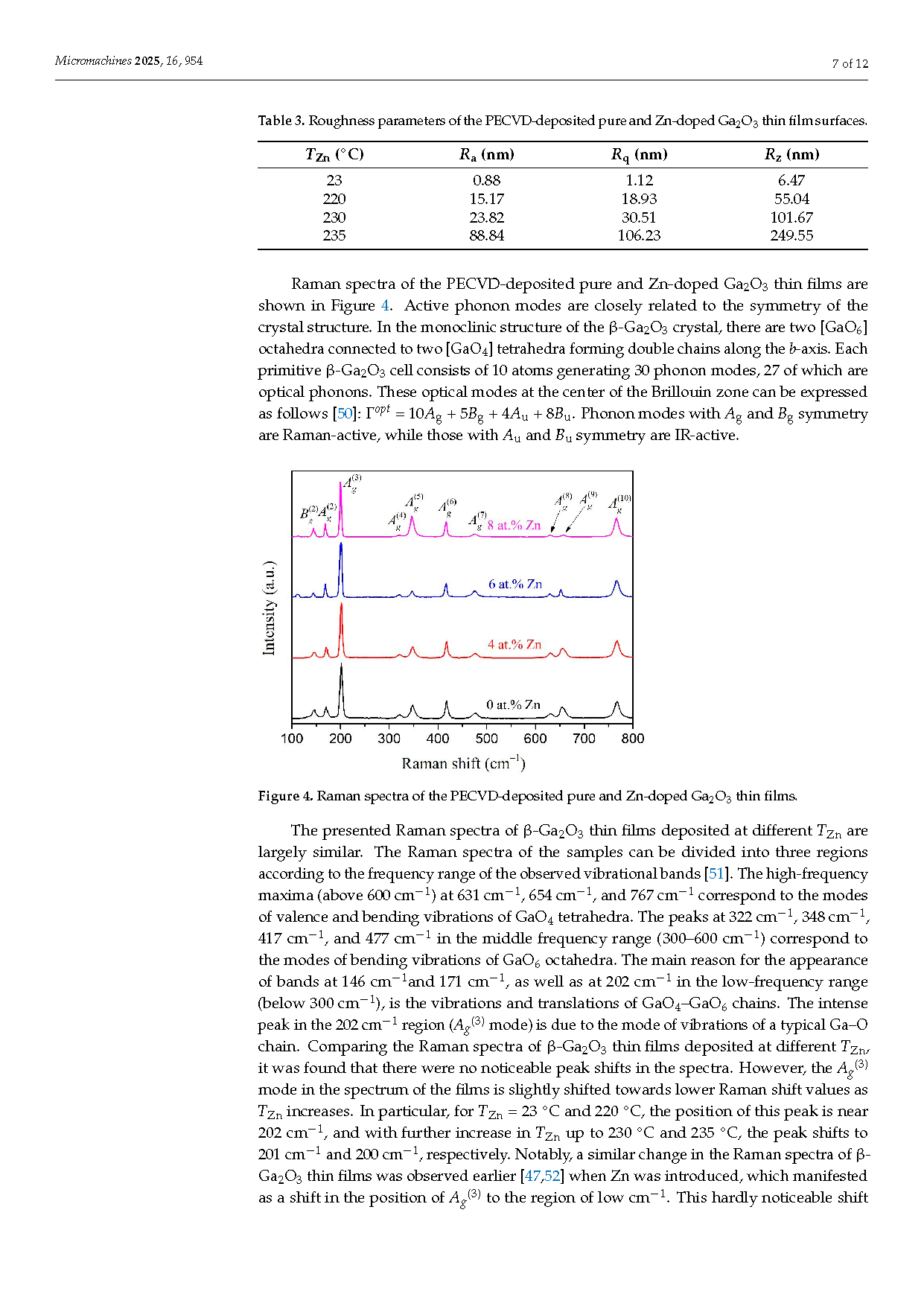
Figure 1. XRD patterns of the PECVD-deposited pure and Zn-doped Ga2O3 thin films.
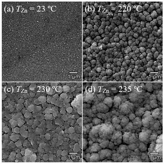
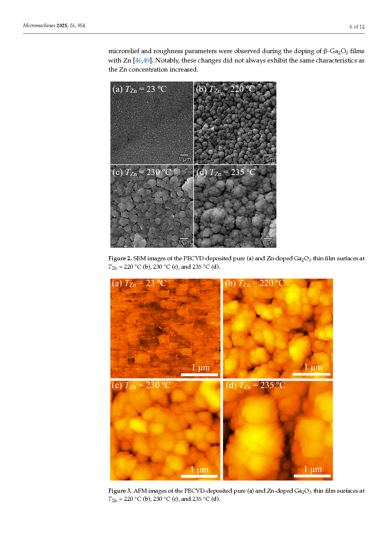
Figure 2. SEM images of the PECVD-deposited pure (a) and Zn-doped Ga2O3 thin film surfaces at TZn = 220 °C (b), 230 °C (c), and 235 °C (d).
DOI:
doi.org/10.3390/mi16080954