Paper Sharing
【Domestic Papers】Investigation on the Thermal Expansion Property of ε-Ga₂O₃ Thin Films Grown by Heteroepitaxy
日期:2025-09-16阅读:669
Researchers from the Sun Yat-Sen University have published a dissertation titled "Investigation on the Thermal Expansion Property of ε-Ga2O3 Thin Films Grown by Heteroepitaxy" in Advanced Engineering Materials.
Project Support
This work was supported by the National Key Research and Development Program of China (grant no. 2023YFF1500700), the Natural Science Foundation of China (grant no. 62074167), the Research and Development Plan Project of Guangdong Province (grant no. 2021B0101300005), and Guangdong Basic and Applied Basic Research Foundation (grant no. 2022B1515120081).
Background
Recently, ε-Ga₂O₃ (κ-Ga₂O₃), a metastable phase of the Ga₂O₃ family, has attracted significant attention due to its ultra-wide bandgap (≈4.9 eV), pronounced spontaneous polarization, and strong piezoelectricity, making it a promising candidate for high-electron-mobility transistors and RF front-end filter devices. However, since ε-Ga₂O₃ lacks a bulk crystal, its growth relies exclusively on heteroepitaxy, where stress control becomes a critical challenge. Inevitably, lattice and thermal mismatches during heteroepitaxy lead to residual stress, which may cause cracking or warping of thin films and severely degrade device performance and reliability. While the crystal structure and lattice constants of ε-Ga₂O₃ have been well established through theoretical and experimental studies, its thermal expansion properties remain unresolved. This knowledge gap significantly hinders stress engineering and epitaxial process optimization. Therefore, developing reliable methods to determine the thermal expansion coefficients of ε-Ga₂O₃ and other non-bulk functional materials is of both scientific importance and practical relevance.
Abstract
The rapid developments of novel functional materials and devices have led to intensified material growth challenges. Notably, stress engineering impacts the entire materials processes from growth, fabrication, to packaging. This article explores the residual stress of ε-Ga2O3 thin film, an emerging wide-bandgap semiconductor lacking a bulk crystal. Herein, temperature-dependent high-resolution X-ray diffraction ω-scan is employed for the curvature measurement, and high tensile stress is observed in all the ε-Ga2O3 samples. Combining Stoney's Equation, the thermal expansion coefficients of ε-Ga2O3 are extracted for the first time to be 10.8 – 11.2 × 10⁻⁶ °C−1 parallel to the (001) plane and 5.03–7.66 × 10⁻⁶ °C−1 perpendicular to (001) plane. Owing to stark differences in thermal mismatch (209% with Si, 54% with sapphire), 700-nm-thick Si-based ε-Ga2O3 exhibits cracking, whereas 1800-nm-thick sapphire-based sample remains crack-free. This work provides new insights into the stress engineering of ε-Ga2O3 and provides a universal thermal expansion measurement method applicable to heteroepitaxial systems of non-bulk functional materials.
Conclusion
In conclusion, the thermal expansion properties of wide-bandgap semiconductor ε-Ga2O3 grown by large thermal mismatch heteroepitaxy are investigated. For the samples grown on c-plane sapphire substrate and Si(111) substrate, high tensile stress is observed. Temperature-dependent curvature measurements are carried out by HRXRD ω-scan based on the models of bilayer structure for ε-Ga2O3/sapphire and trilayer structure for ε-Ga2O3/AlN/Si(111). For ε-Ga2O3, the TEC on the biaxial (001) plane, α‖ε-Ga2O3, is extracted to be 10.8–11.2 10 6°C 1, while the TEC perpendicular to the (001) plane, α⊥ε-Ga2O3, is extracted to be 5.03– 7.66 10 6 °C 1.Theseresults indicate a thermal mismatch of 54% for ε-Ga2O3 grown on sap phire and 209% for ε-Ga2O3 grown on Si. Cracks are observed in the Si-based ε-Ga2O3 film with a thickness of 700 nm, while there is no crack in the sapphire-based ε-Ga2O3 film with a thickness of 1800nm,demonstrating the larger thermal mismatch between ε-Ga2O3 and Si. The accurate determination of TEC not only pro vides an insight into the basic thermal expansion property but also offers crucial guidance for stress engineering in the hetero epitaxy of ε-Ga2O3.
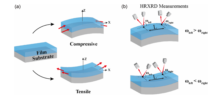
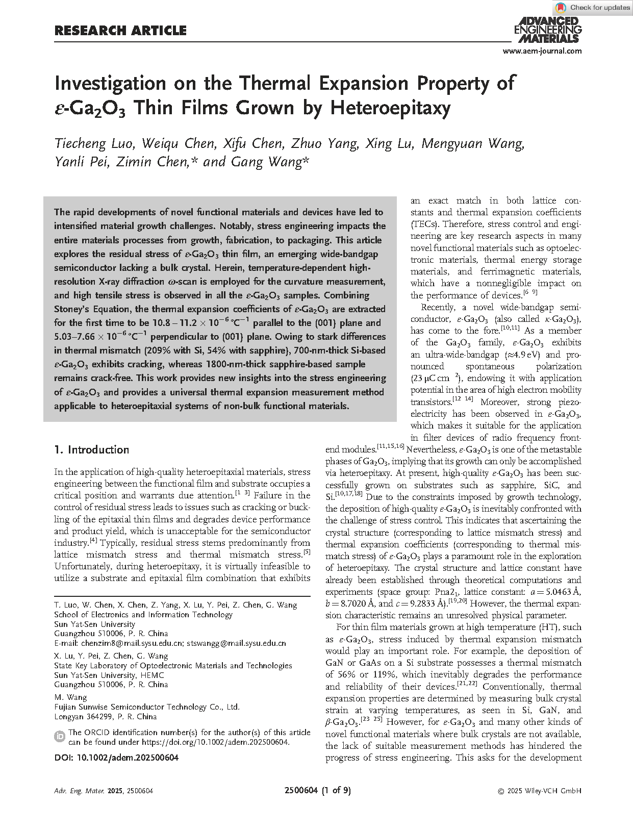
Figure 1. a) The stress state between heteroepitaxial films and substrates can lead to wafer bowing. b) The model of ex situ HRXRD curvature measure ments. L represents the horizontal distance between the two points of the ω-scan measurement. The curvature is determined by κ=1/R≈(ωr-ωl)/|L|.
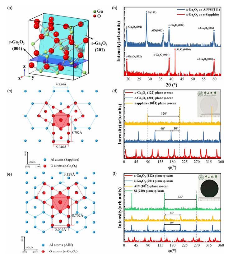
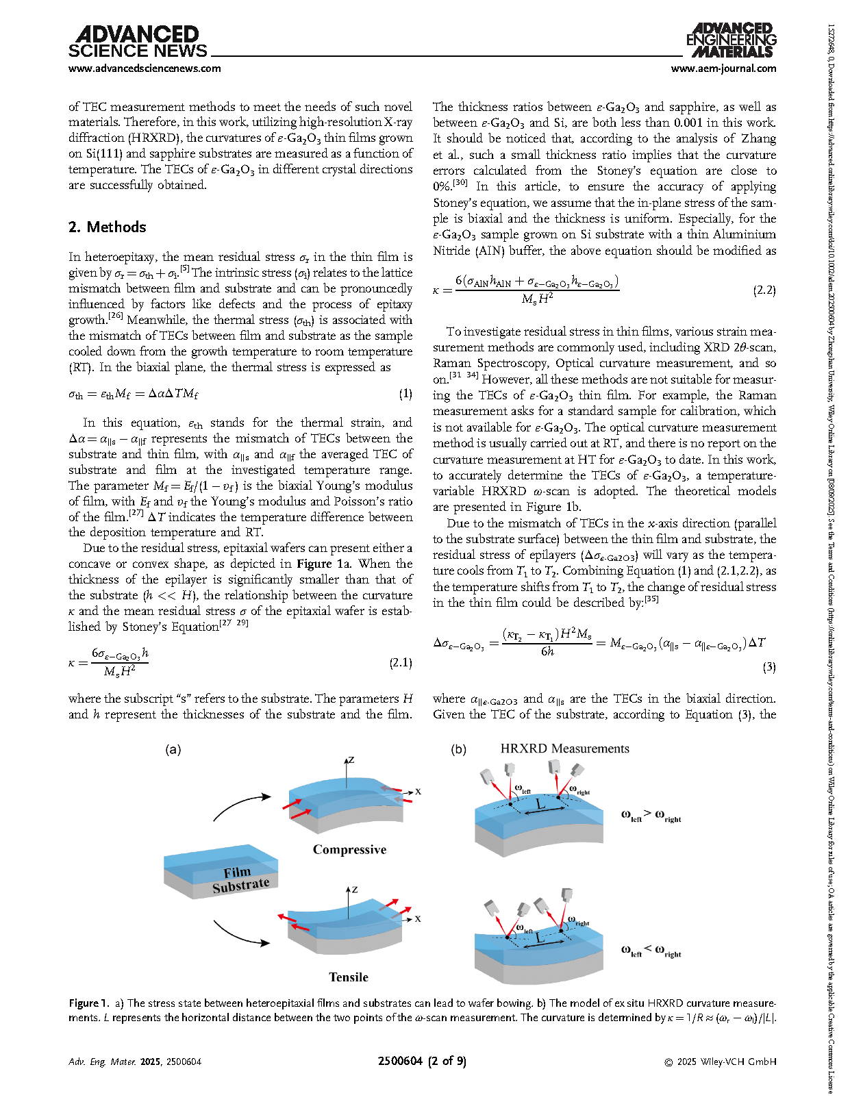
Figure 2. a) The crystal structure of orthorhombic ε-Ga2O3, b) 2θ-scan patterns of ε-Ga2O3 films grown on c-plane sapphire and Si(111). Schematic diagrams illustrating the epitaxial relationship and the 120° in-plane rotational domains for orthorhombic ε-Ga2O3 on c) c-sapphire and e) AlN/Si(111). The red shaded hexagons represent the equivalent pseudohexagonal ε-Ga2O3. Phi-scan patterns of ε-Ga2O3 films grown on d) c-sapphire and f) AlN/ Si(111). Diffractions of the asymmetric (122) and (201) planes of ε-Ga2O3, the (10-14) plane of the c-sapphire substrate, the (220) plane of the Si substrate, and the (10-15) plane of AlN are presented. The photos of the two samples are shown in the inset of (d) and (f).
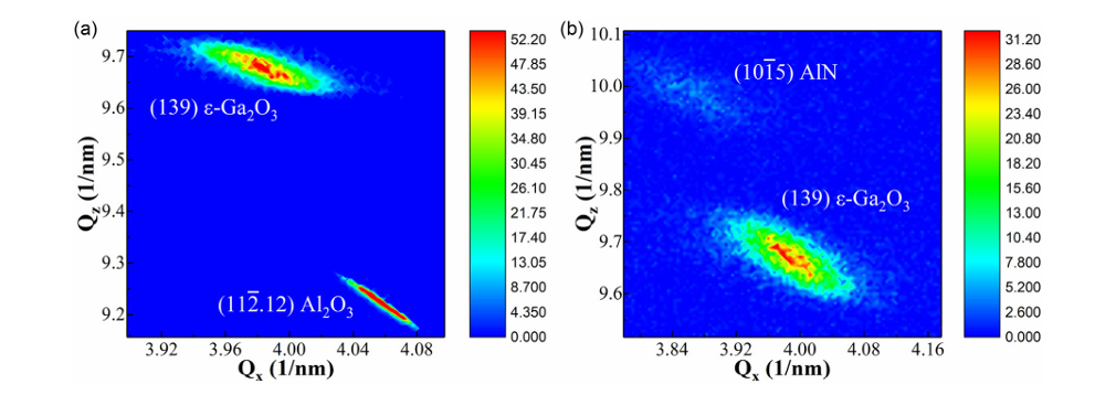
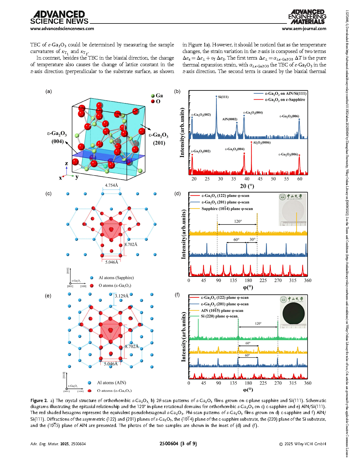
Figure 3. RSM around ε-Ga2O3(139) grown on a) c-sapphire and b) AlN/Si(111).
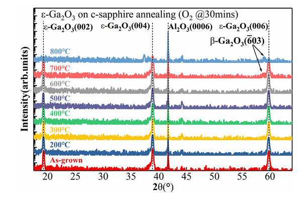
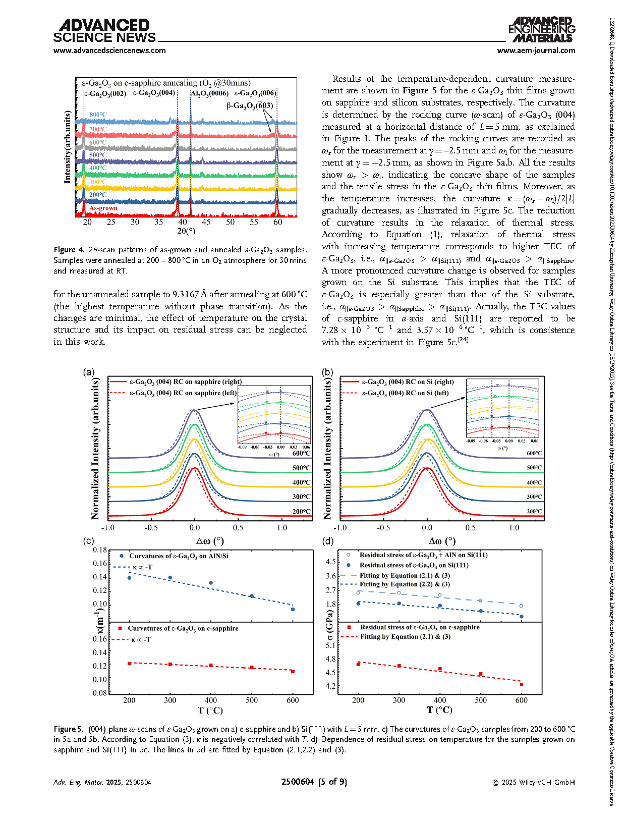
Figure 4. 2θ-scan patterns of as-grown and annealed ε-Ga2O3 samples. Samples were annealed at 200– 800°C in an O2 atmosphere for 30 mins and measured at RT.
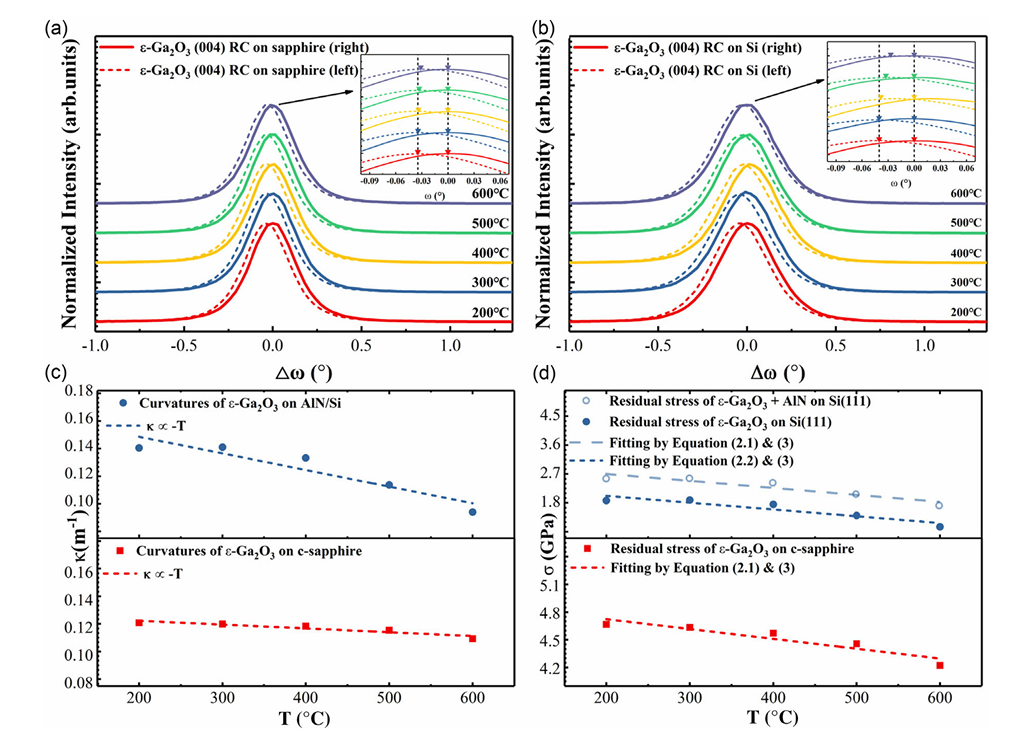
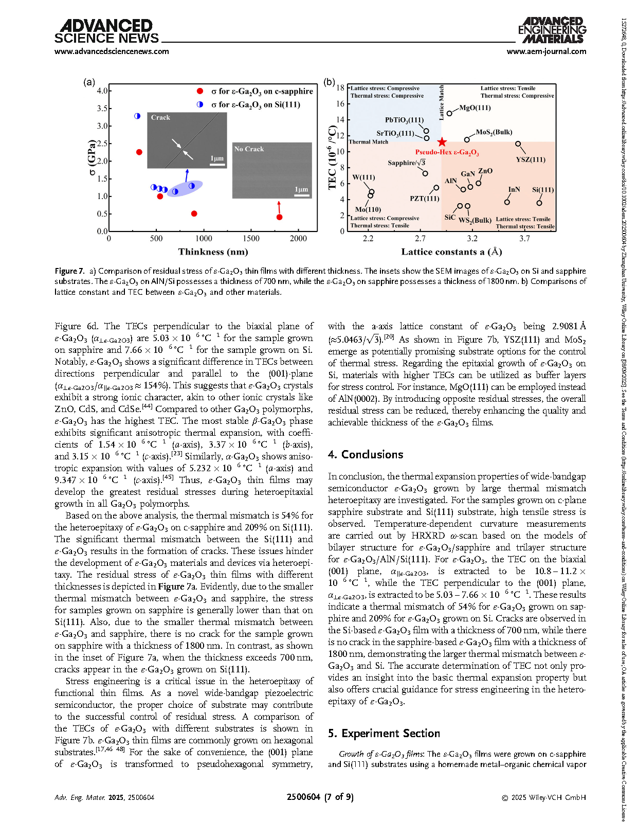
Figure 5. (004)-plane ω-scans of ε-Ga2O3 grown on a) c-sapphire and b) Si(111) with L= 5mm. c) The curvaturesof ε-Ga2O3 samplesfrom 200to 600°C in 5a and 5b. According to Equation (3), κ is negatively correlated with T. d) Dependence of residual stress on temperature for the samples grown on sapphire and Si(111) in 5c. The lines in 5d are fitted by Equation (2.1,2.2) and (3).
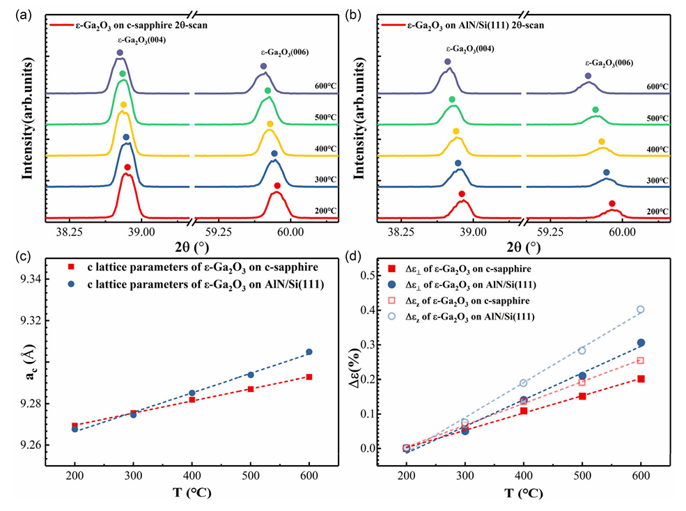
Figure 6. 2θ-scans of ε-Ga2O3 with temperature ranging from 200 to 600°C on a) c-sapphire and b) Si(111). c) The lattice parameters ac of ε-Ga2O3 epitaxial films extracted from Figure 6a,b, according to Bragg’s Law 2 d sinθ=n λ. The line in 6c is a guide for the eyes. d) The strain variation in the z direction of ε-Ga2O3 from 200 to 600°C based on the lattice parameters in Figure 6c. The lines in 6c are fit according to Equation (4), i.e., Δε⊥=Δεz- υε-Ga2O3 (α‖s- α‖ε-Ga2O3) ΔT.
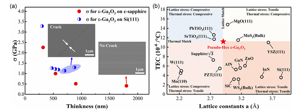
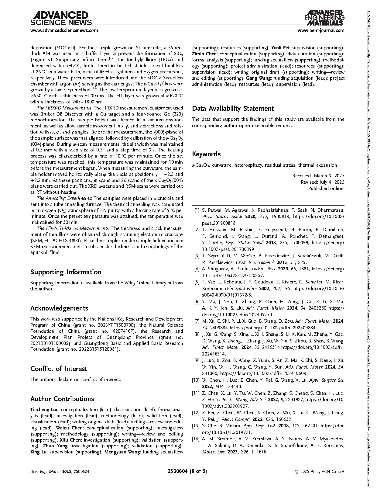
Figure 7. a) Comparison of residual stress of ε-Ga2O3 thin films with different thickness. The insets show the SEM images of ε-Ga2O3 on Si and sapphire substrates. The ε-Ga2O3 on AlN/Si possessesa thickness of 700nm, while the ε-Ga2O3 onsapphire possessesa thickness of 1800nm.b) Comparisonsof lattice constant and TEC between ε-Ga2O3 and other materials.
DOI:
doi.org/10.1002/adem.202500604