Paper Sharing
【International Papers】Fabrication of β-Ga₂O₃/air-gap structures on (001) β-Ga₂O₃ using HCl gas etching
日期:2025-09-17阅读:607
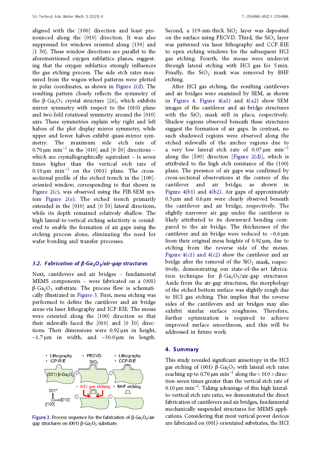
Researchers from the National Institute for Materials Science have published a dissertation titled "Fabrication of β-Ga2O3/air-gap structures on (001) β-Ga2O3 using HCl gas etching" in Science and Technology of Advanced Materials: Methods.
Background
β-Ga2O3 is an emerging wide bandgap semiconductor with great potential for a wide range of applications. It offers both a high critical breakdown field of nearly 8 MV cm−1 and compatibility with melt growth techniques for producing high-quality, scalable wafers. Owing to these two major advantages over conventional wide bandgap semiconductors – such as SiC, GaN, and diamond—β-Ga2O3 is increasingly regarded as a promising material for next-generation low-loss, high-voltage power devices. In addition, β-Ga2O3 demonstrates native solar-blind photoresponsivity and gas sensitivity, which are beneficial for developing filterless solar-blind photodetectors and gas sensors, respectively. It also possesses favorable mechanical properties, including a high Young’s modulus (~261 GPa) and a high acoustic velocity (~6623 m s−1), both comparable to those of Si, rendering it well-suited for microelectromechanical systems (MEMS) applications. These properties suggest that β-Ga2O3 could serve as a highly versatile platform for future electromechanically coupled and tunable devices in electronics, optoelectronics, and advanced sensing. Potential applications include radio-frequency MEMS components in high-power, high-frequency systems for defense, wireless infrastructure, satellites, and resonance-enhanced solar-blind UV photodetectors and gas sensors.
Abstract
β-Ga2O3/air-gap structures were fabricated on (001) substrates via crystallographic etching with HCl gas. Etching at 650 °C under an HCl partial pressure of 250 Pa resulted in a vertical etch rate of 0.10 μm/min on the (001) plane and a lateral etch rate of 0.70 μm/min along the < 010 > direction. This high orthogonal etching anisotropy enabled the formation of β-Ga2O3/air-gap structures – such as cantilevers and air bridges – without the need for wafer bonding or transfer processes. This straightforward technique, compatible with commonly used (001) substrates, holds promise for the integration of β-Ga2O3-based microelectromechanical systems (MEMS) and power electronic devices.
Conclusion
This study revealed significant anisotropy in the HCl gas etching of (001) β-Ga2O3 with lateral etch rates reaching up to 0.70 µm min−1 along the < 010 > direction-seven times greater than the vertical etch rate of 0.10 µm min−1. Taking advantage of this high lateral-to-vertical etch rate ratio, we demonstrated the direct fabrication of cantilevers and air bridges, fundamental mechanically suspended structures for MEMS applications. Considering that most vertical power devices are fabricated on (001)-orientated substrates, the HCl gas etching method presented here is particularly promising for the monolithic integration of MEMS and power devices.
Lastly, it is worth noting that a variety of crystallographic anisotropic etching techniques have been reported for β-Ga2O3, including hot phosphoric acid etching, photoelectrochemical etching, metal-assisted chemical etching, hydrogen-environment anisotropic thermal etching, forming gas etching, Ga flux etching, triethylgallium gas etching, and tert-butyl chloride gas etching. Although our study focused on HCl gas etching, the air-gap formation demonstrated here might also be achievable using these alternative methods. However, further investigation should be required – particularly to determine the conditions under which the lateral etching rate becomes sufficiently high relative to the vertical etching rate.
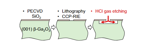
Figure 1. Process sequence for selective-area HCl gas etchingon the (001) β-Ga2O3 substrate.
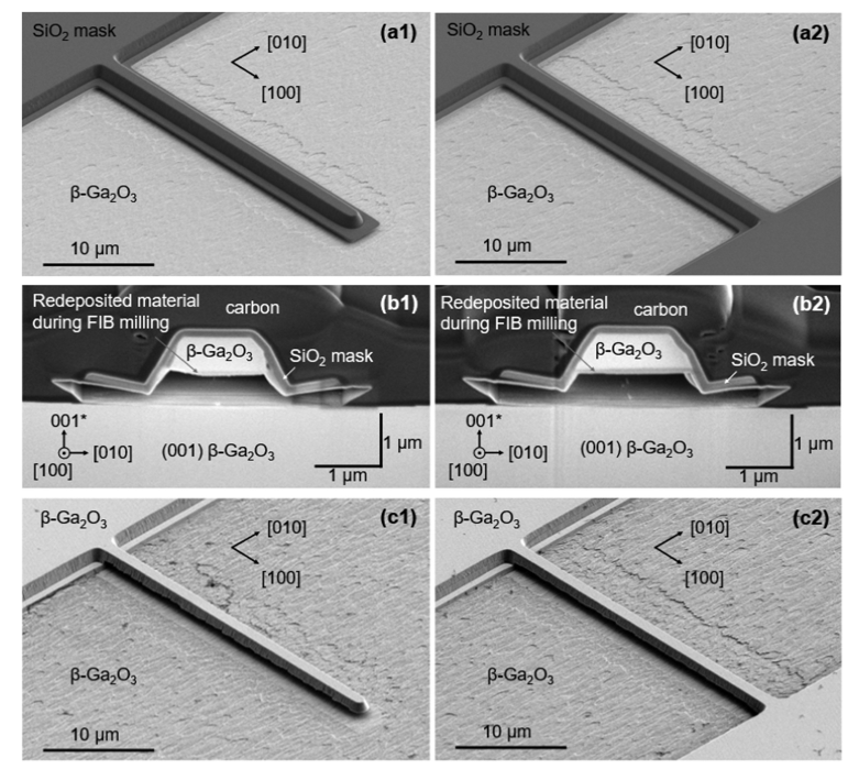
Figure 2. Summary of 54° tilted-view SEM images of the fabricated (a1)–(c1) cantilever and (a2)–(c2) air bridge structures on (001) β-Ga2O3 substrates. Images (a1) and (a2) were acquired after etching with HCl gas. Images (b1) and (b2) show cross-sectionalviews corresponding to (a1) and (a2), respectively. Images (c1) and (c2) were taken after the removal of the SiO2 mask.
DOI:
doi.org/10.1080/27660400.2025.2554046