Paper Sharing
【International Papers】Monolithically Integrated RTL-Based Inverters for Gate Driver IC Using β-Ga₂O₃ MOSFETs
日期:2025-09-18阅读:564
Researchers from the King Abdullah University of Science and Technology (KAUST) have published a dissertation titled "Monolithically Integrated RTL-Based Inverters for Gate Driver IC Using β-Ga2O3 MOSFETs" in IEEE Transactions on Electron Devices.
Background
β-Ga2O3 possesses excellent power electronic figures of merit and economically feasible wafer fabrication, driving significant progress toward high-performance devices and approaching commercial viability. The next step is the development of integrated circuits for power switching, where monolithic integration of gate drivers with power MOSFETs can reduce parasitics and enhance switching speed and stability. Due to the lack of high-performance p-channel devices, β-Ga2O3 logic circuits adopt topologies similar to GaN, with RTL offering a simple and practical solution. While prior studies demonstrated device potential, challenges remain in achieving high-frequency, high-power gate drivers, making the development of monolithically integrated β-Ga2O3 gate driver ICs a critical step toward commercialization.
Abstract
The gate driver interfaces power MOSFETs with digital control circuits by providing the necessary drive current for rapid switching. This work demonstrates a monolithically integrated gate driver integrated circuit (IC) based on β-Ga2O3 resistor-transistor logic (RTL) inverter, utilizing enhancement-mode multifinger (MF) MOSFETs and recessed epitaxy-based resistors. The 0.785-mm2 chip integrates two RTL inverters in a noninverting configuration and achieves voltage gains of 11.9 and 12.2 V/V with high/low noise margins of 3.4 /1.3 V and 3.0/1.6 V at a 15-V supply. Dynamic characterization shows a switching speed of 9.4 μs with a 5-V control input, producing output swings up to 15 V. These results validate the suitability of RTL-based gate drivers for β-Ga2O3 power ICs and highlight their potential for scalable monolithic integration.
Conclusion
A monolithically integrated RTL-based gate driver IC using β-Ga2O3 enhancement-mode MOSFETs and recessed epitaxy-based resistors was designed, fabricated, and characterized. RTL inverters achieved voltage gains exceeding 12 V/V, with robust noise margins and cascaded operation. Static characterization revealed high ON/OFF current ratios (>109), VTH of 2.4 V, and RON,sp of 16.8 m·cm2.
Dynamic switching measurements demonstrated rise/fall times of 4.8/4.6 µs and a maximum switching frequency of 106.4 kHz, with performance governed by MOSFET capacitances and interconnect parasitics. C–V analysis highlighted the drain-bias dependence of gate-to-drain capacitance, while breakdown voltages near 150 V confirmed device robustness. These results validate the potential of RTL-based architecture for compact, high-voltage β-Ga2O3 power ICs and lay the groundwork for scalable monolithic integration in ultra-wide bandgap electronics.
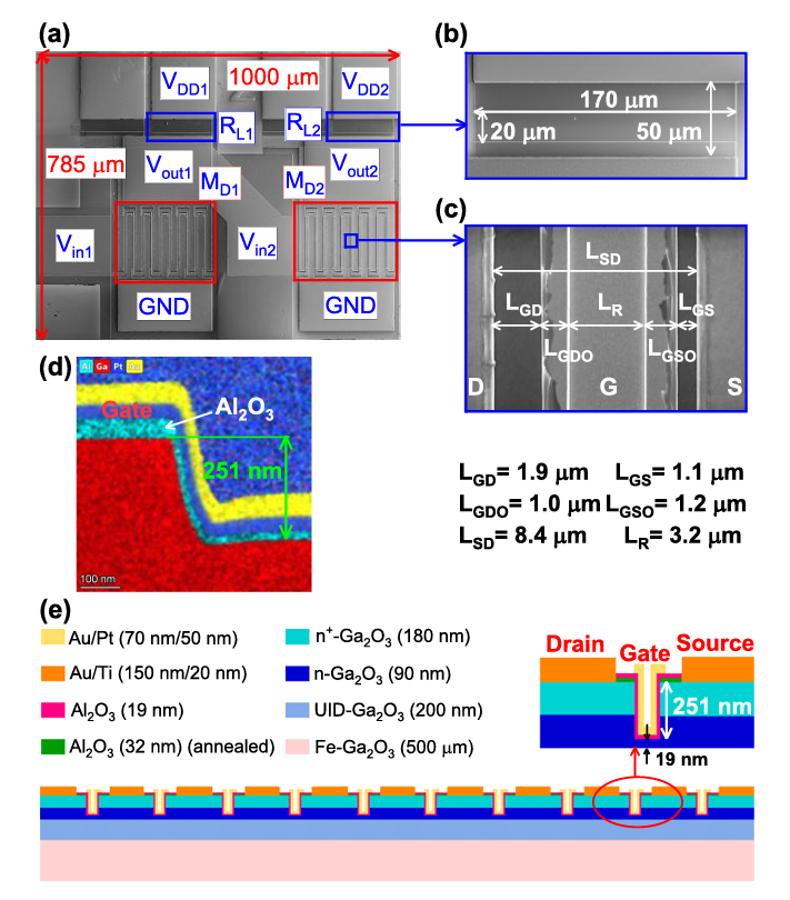
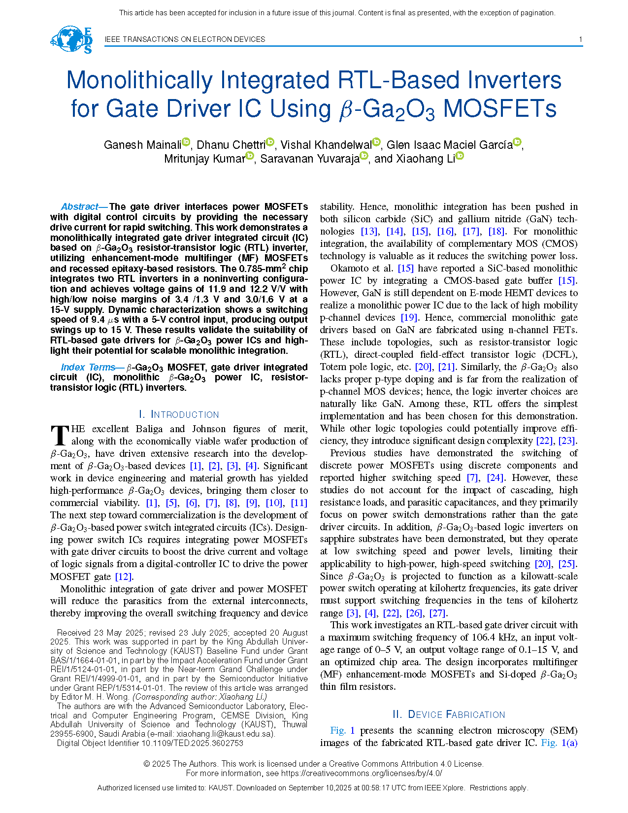
Fig. 1. (a) SEM image of the fabricated gate driver IC. (b) Enlarged view showing the dimensions of the resistor. (c) Enlarged view showing the dimensions of the gate region. (d) EDX mapping in a TEM image of the recess region of the MF MOSFET, showing the spatial distribution of elements. (e) Cross-sectional schematic of the MF MOSFET highlighting different epitaxial layers.
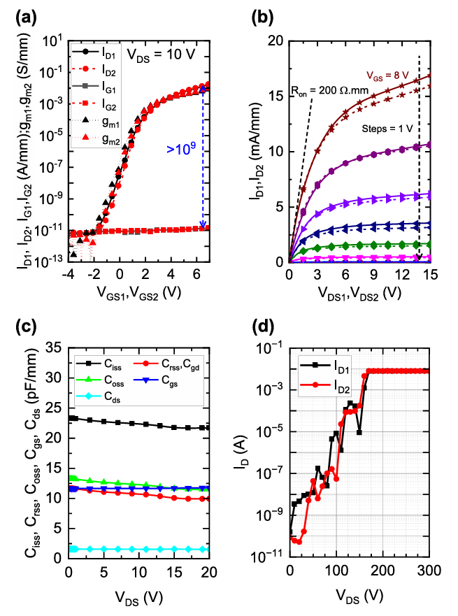
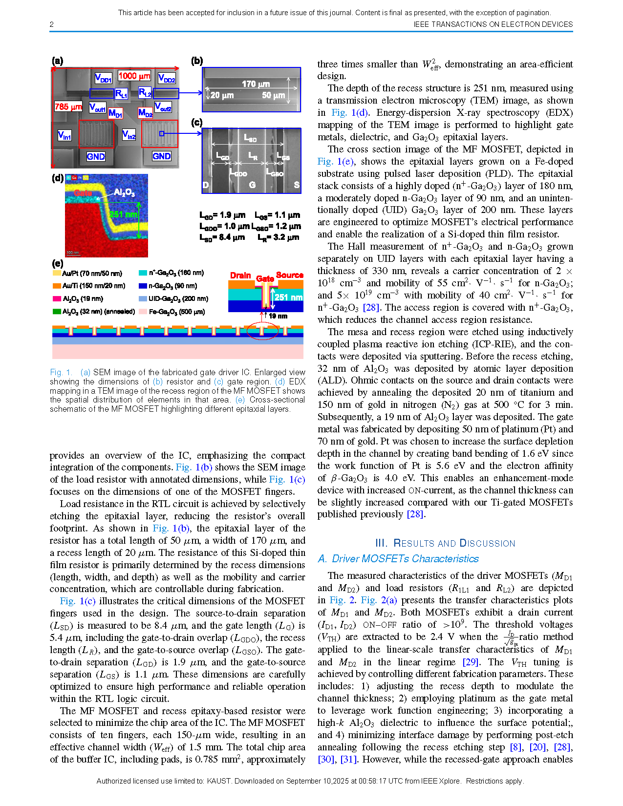
Fig. 2. (a) Transfer characteristics of MD1 (solid line) and MD2 (short dashed line). (b) Output characteristics of MD1 (solid line) and MD2 (short dashed line). (c) Capacitance versus VDS plot of an MF MOSFET. (d) Breakdown voltage measurement of MF MOSFETs.
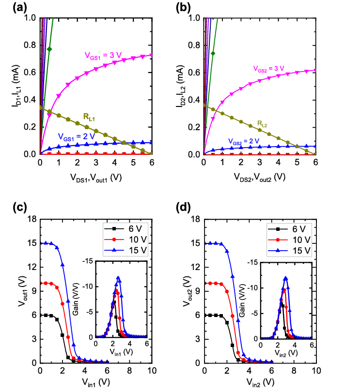
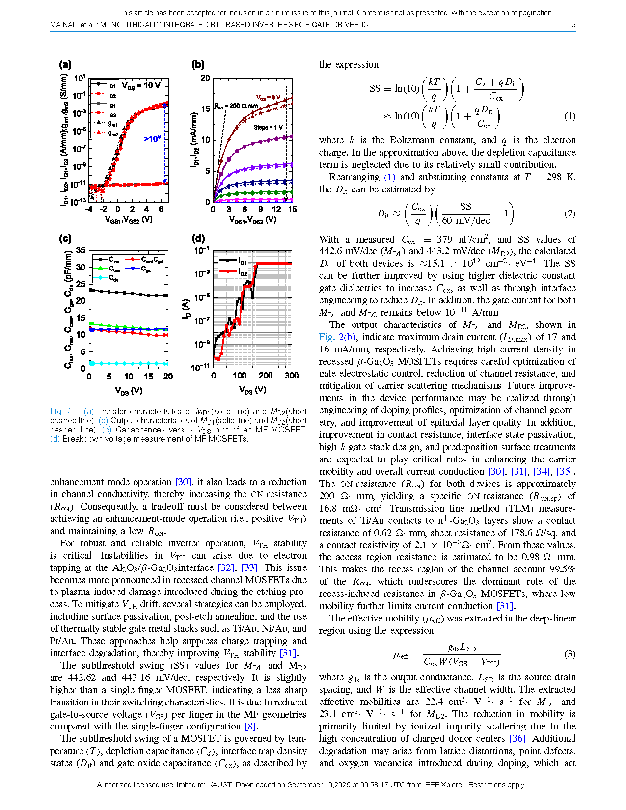
Fig. 3. (a) Load-line plot for RTL1. (b) Load-line plot for RTL2. (c) Transfer characteristics and gain plot (inset) of the RTL1 inverter. (d) Transfer characteristics and gain plot (inset) of the RTL2 inverter.
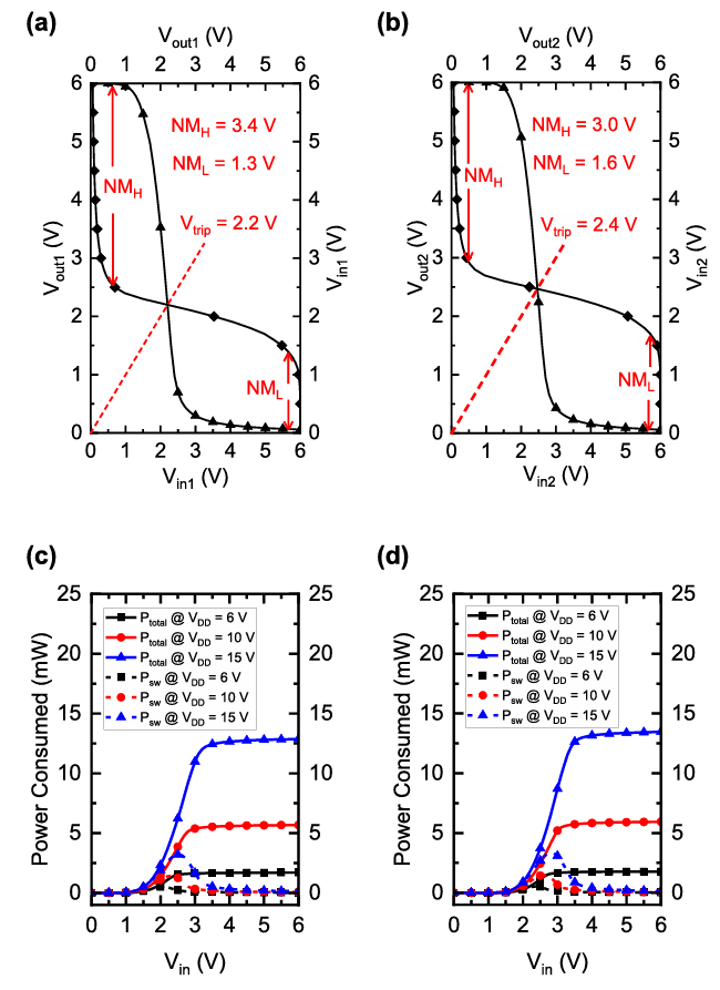
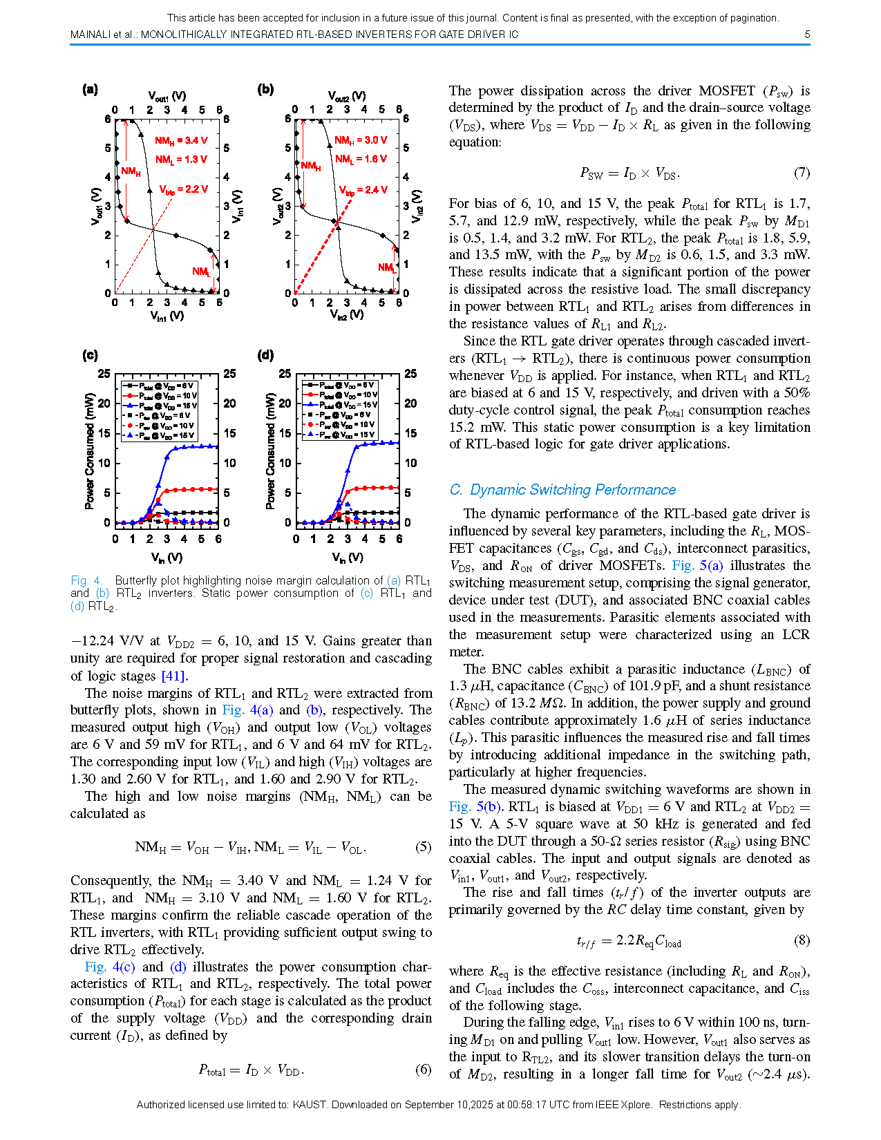
Fig. 4. (a) Butterfly plot highlighting noise margin calculation of the RTL1 inverter. (b) Butterfly plot highlighting noise margin calculation of the RTL2 inverter. (c) Static power consumption of the RTL1 inverter. (d) Static power consumption of the RTL2 inverter.
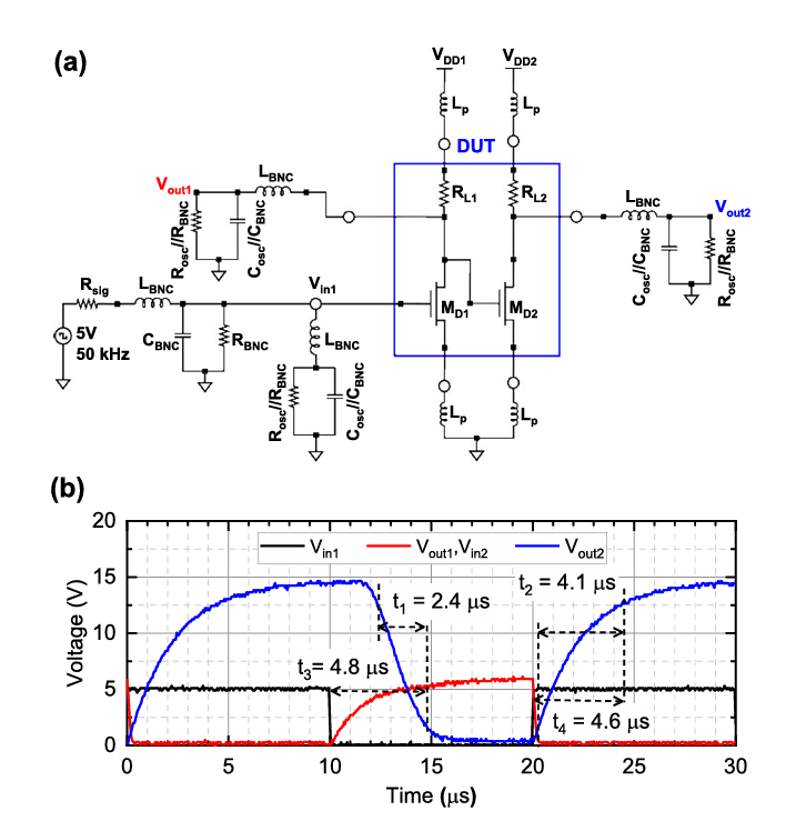
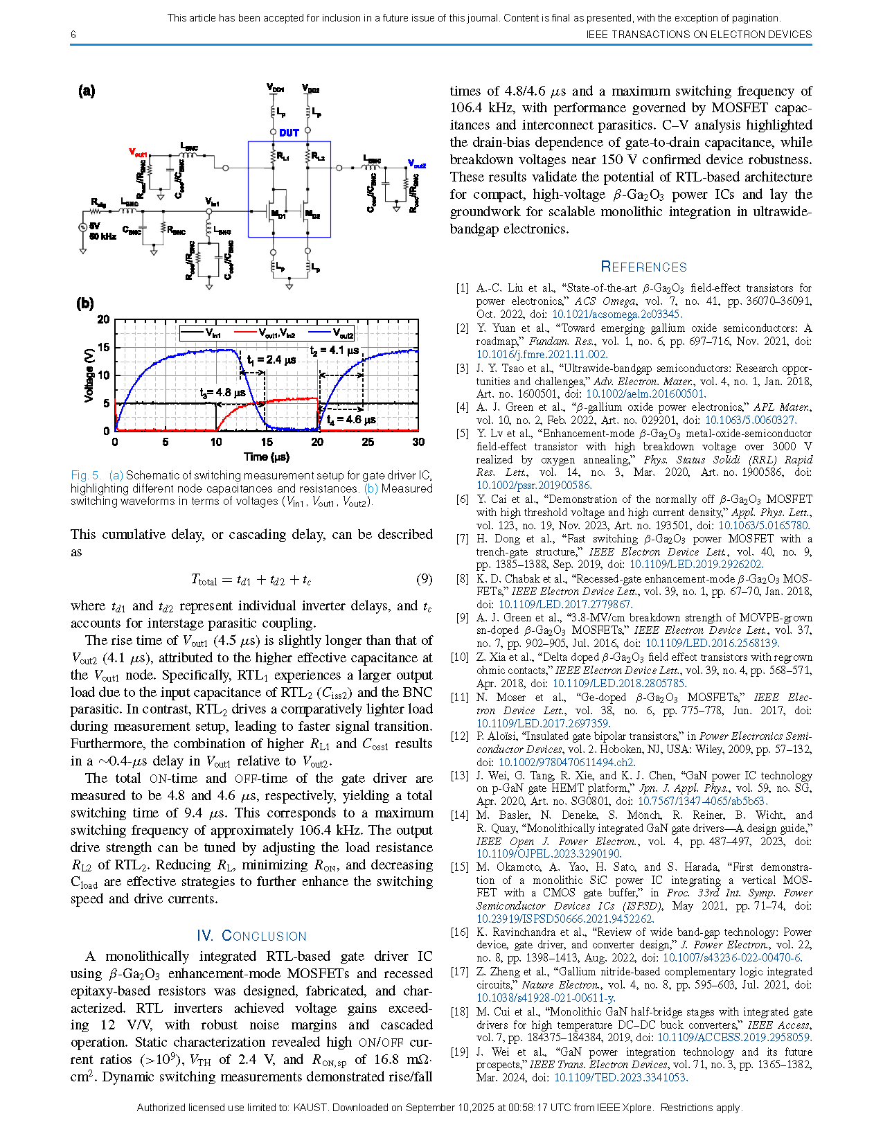
Fig. 5. (a) Schematic of the switching measurement setup for the gate driver IC, highlighting different node capacitances and resistances. (b) Measured switching waveforms in terms of voltages (Vin1, Vout1, Vout2).
DOI:
doi.org/10.1109/TED.2025.3602753