Paper Sharing
【Domestic Papers】Low Von β -Ga₂O₃ Schottky Diodes With Synergistic Suppression of Bulk and Perimeter Leakage
日期:2025-09-19阅读:562
Researchers from the School of Microelectronics have published a dissertation titled "Low Von β-Ga2O3 Schottky Diodes With Synergistic Suppression of Bulk and Perimeter Leakage" in IEEE Electron Device Letters.
Project Support
This work was supported by the National Key Research and Development Program of China (Grant No. 2024YFE0205200), the Provincial Science and Technology Major Project of Jiangsu (Grant No. BG2024030), the National Natural Science Foundation of China (Grant Nos. U23A20358, 62234007, 62474170, and 61925110), and the JieBang Headed Project of Changsha City, Hunan Province (Grant No. kq2301006). The authors also acknowledge the support from the Center for Micro and Nanoscale Research and Fabrication of University of Science and Technology of China (USTC).
Background
Power semiconductor devices are evolving toward higher efficiency, lower energy consumption, and miniaturization, which drives the rapid adoption of wide-bandgap materials. Among them, β-Ga₂O₃ has emerged as a strong contender for next-generation high-power electronics owing to its wide bandgap (4.5–4.9 eV), higher Baliga’s figure of merit compared with SiC and GaN, and the potential for low-power dissipation in unipolar devices. In addition, cost-effective melt growth and high-quality epitaxy make large-scale commercialization feasible. In recent years, β-Ga₂O₃-based power diodes have seen significant progress, with Schottky barrier diodes (SBDs) being at the forefront. However, achieving both low on-state loss and low off-state loss remains a critical challenge. The on-state performance can be improved by thinning epitaxial layers and substrates, inserting TiO₂ interlayers, or using low work-function anodes to reduce the turn-on voltage (Von). In contrast, the off-state loss is often dominated by leakage currents: perimeter leakage caused by edge electric-field crowding and bulk leakage induced by poor carrier blocking capability of low-barrier contacts, barrier lowering, and tunneling under reverse bias. Various termination structures, such as field plates, junction termination extension, high-resistive or mesa terminations, have been proposed to mitigate edge-related leakage, while high-barrier metals or RESURF techniques have been applied to suppress bulk leakage. Nevertheless, there exists an inherent trade-off between achieving a low Von and maintaining strong blocking capability. Inspired by the RESURF concept, a dual-barrier design can be introduced, where the high-barrier region pinches off or shields the low-barrier region under reverse bias to suppress bulk leakage, while the low-barrier region conducts first under forward bias to maintain low Von. Building on this principle, this work demonstrates trench Schottky barrier controlled Schottky diodes (TSBSDs), in which PtOx and W form high and low Schottky barriers with β-Ga₂O₃, respectively. By further integrating composite mesa and junction termination extension (MJTE) structures, both bulk and perimeter leakage are synergistically suppressed, enabling diodes that achieve a low turn-on voltage of 0.71 V along with a high breakdown voltage of 1466 V.
Abstract
This work first presents β-Ga2O3 trench Schottky barrier controlled Schottky diodes (TSBSDs) with low turn-on voltage (Von) and substantially improved block ing performance. The high Schottky barrier formed by PtOx and β-Ga2O3 in the trench region can pinch off and shield ehe tungsten (W) contact region with low barrier, thereby effectively suppressing reverse bulk leakage. In addition, the composite mesa and junction termination extension (MJTE) is used to alleviate the perimeter leakage caused by edge electric field crowding. The fitting and analysis of leakage current versus radius in logarithmic scale is demonstrated to identify the location that dominates leak age. As a result, the leakage is reduced by more than three orders of magnitude owing to the synergistic suppression of bulk and perimeter leakage. Meanwhile, the breakdown voltage increases from 458 V to 1466 V, with a low Von maintained at 0.71 V. In additionally, the TSBSD featuring MJTE maintains the lowest power loss in most duty cycles benefiting from the low Von and leakage current. This work paves the way to improve the operational efficiency of β-Ga2O3 Schottky diodes.
Conclusion
We achieve a balanced trade-off between low Von and high Vbr through the synergistic suppression of perimeter and bulk leakage. The leakage location is effectively identified by fitting the relationship between leakage and device dimensions, which proves valuable for the research community. A TSBS structure utilizing two distinct Schottky barriers is introduced for the first time to reduce bulk leakage while preserving low Von. As a result, the Vbr increases by 3.2 times, PFOM rises sevenfold, and PL drops by 50%, providing a clear pathway for advancing high-efficiency power devices.
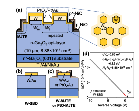
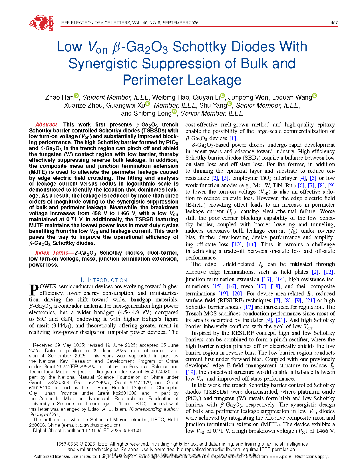
Fig. 1. (a) Schematic view of β-Ga2O3 TSBSD-MJTE and its anode layout. Device structure of the (b) W-SBD and (c) W-MJTE or PtO-MJTE. (d) Nd-Na and qΦB extracted by 1/C2-V.
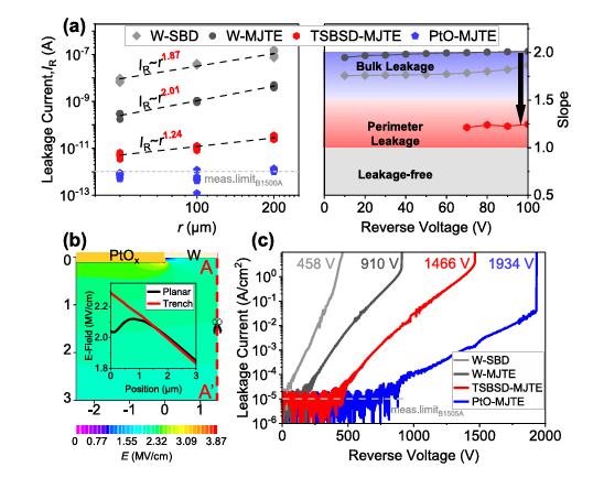
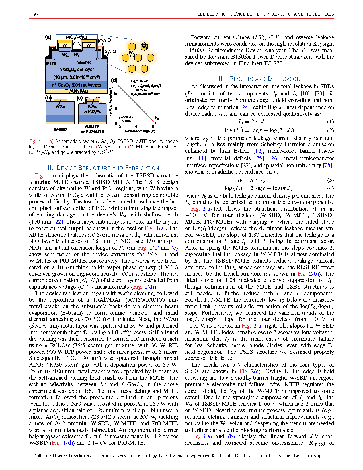
Fig. 2. (a) Dependence of IR onr at-100V(left), and the variation of the log(IR)/log(r) slope from 0 V to-100 V (right) for different SBDs. (b) The RESURF effect of TSBS structure under-1500 V. (c) Comparison of breakdown characteristics for devices with different structures.
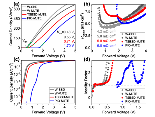
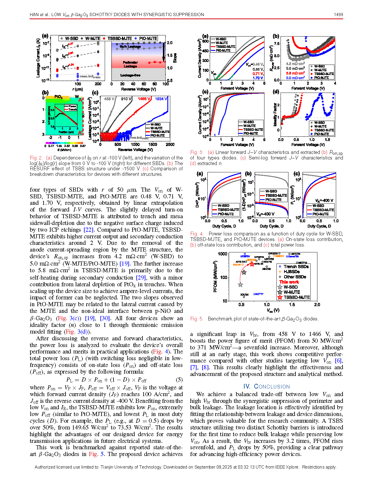
Fig. 3. (a) Linear forward J–V characteristics and extracted (b) Ron,sp of four types diodes. (c) Semi-log forward J–V characteristics and (d) extracted n.
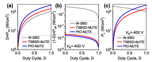
Fig. 4. Power loss comparison as a function of duty cycle for W-SBD, TSBSD-MJTE, and PtO-MJTE devices. (a) On-state loss contribution, (b) off-state loss contribution, and (c) total power loss.
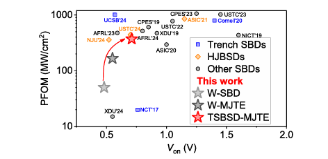
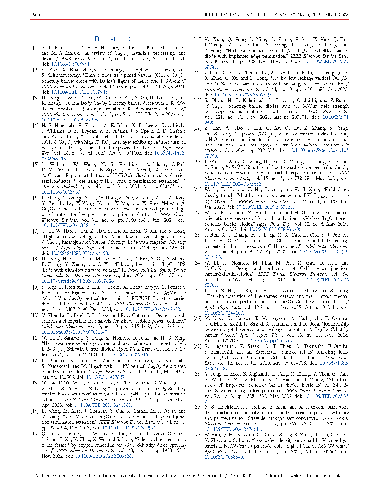
Fig. 5. Benchmark plot of state-of-the-art β-Ga2O3 diodes.
DOI:
doi.org/10.1109/LED.2025.3584109