


Discover
【Knowledge Discover】Core Technology of Semiconductor Epitaxial Growth: Growth Mechanism and Equipment Principle
日期:2025-09-19阅读:2161
PART01
Definition and Core Values of Epitaxial Technology
Epitaxy, derived from the combination of the Greek words "Epi" (on top) and "taxis" (arranged), specifically refers to the precise process of growing a single crystal film along its crystal direction on a single crystal substrate. The grown epitaxial layer maintains a consistent crystal orientation and lattice structure with the substrate, and the thickness (micrometer level), doping concentration and crystal quality can be precisely regulated through atomic-level control to form the core structure of "epitaxial sheet = substrate + epitaxial layer".
Epitaxy can be divided into homogeneous epitaxy (such as Si on Si) and heterogeneous epitaxy (such as GaAs on Si) based on material similarities and differences. The former ensures lattice matching, while the latter expands the possibility of material combinations and lays the foundation for the fabrication of multifunctional devices.
1) Limitations of bulk single crystal materials and breakthroughs in epitaxial technology
There are two core bottlenecks in traditional bulk single crystal materials:
First, the defect density is high, and lattice defects such as dislocations and vacancies tend to form during natural growth, which adversely affects carrier mobility.
Second, the resistivity is non-uniform, making it difficult to simultaneously satisfy the conflicting requirements of devices for high breakdown voltage (requiring high resistivity) and low series resistance (requiring low resistivity).
Epitaxial technology achieves breakthroughs through the following mechanisms:
Atomic-Level Growth Control: Techniques such as gas-phase epitaxy (e.g., HVPE) allow atoms are arranged in an orderly manner along the substrate lattice, significantly reducing defect density. For example, the crystal integrity of silicon epitaxial layers is much higher than that of bulk silicon, allowing for thickness error control within ±2%;
Precise Doping Control: By changing the proportion of doping gas during the epitaxial process, epitaxial layers with different resistivity can be grown on the same substrate, resolving the "high voltage - low resistance" contradiction of bipolar transistor collectors while eliminating the "latch-up effect" of CMOS devices.
Core Value: From Material Optimization to Device Performance Leap
The core value of epitaxial technology lies in the all-round reconfiguration of semiconductor device performance, which includes three dimensions:
① Solving the physical contradiction of the device: By applying compressive stress to the channel of PMOS devices through selective epitaxy (such as SiGe source-drain epitaxy), the hole mobility increases by more than 30%; In power devices, the coordinated control of epitaxial layer thickness and resistivity can meet the requirements of high-voltage applications above 600V.
② Expand the application boundaries of materials: For third-generation wide bandgap semiconductors such as GaN and SiC, epitaxy is the core link to unlock their performance. For example, GaN heteroepitaxy needs to overcome the 16.9% lattice mismatch with the substrate, control the dislocation density below 10⁸/cm² through the buffer layer design, and make the electron saturation drift velocity exceed 2×10⁷ cm/s to meet the high-frequency requirements of 5G base stations.
③ Reducing manufacturing costs and enhancing reliability: Silicon-based GaN epitaxy technology reduces material costs to 1/20 by replacing expensive SiC substrates with 8-12-inch silicon substrates while being compatible with existing CMOS production lines; For every order of magnitude reduction in epitaxial defect density (such as from 10³/cm² to 10²/cm²), the life reliability of IGBT modules can be increased. by 40%.
The irreplaceability of third-generation semiconductor epitaxy: In scenarios such as new energy vehicle inverters (where the cost of the SiC epitaxial layer accounts for 20% of the total chip cost) and high-speed rail power supplies (where the high-frequency characteristics of GaN reduce energy consumption by 30%), the crystal quality of the epitaxial layer directly determines the device yield and long-term stability. It has become a "must-have process" for high-temperature (>300 ° C), high-frequency (>10 GHz), and high-power (>1000 V) applications.
Epitaxial technology, by deeply integrating material preparation with device manufacturing processes, not only resolves the inherent defect of bulk single crystal materials but also becomes the core engine for breaking through the performance limits of semiconductors. From traditional silicon-based chips to third-generation wide bandgap devices, the "performance Buff" effect of the epitaxial layer runs through the entire process of semiconductor industry upgrading, supporting technological breakthroughs in frontier fields such as new energy vehicles and quantum computing.
PART02
Comparison of Types and Characteristics of Epitaxial Growth
Epitaxial growth can be classified into four types based on differences in material composition, lattice fit, and stress state: homogeneous epitaxy, heterogeneous epitaxy, strain epitaxy, and non-strain epitaxy, each with significant differences in technical characteristics and application scenarios. The following is a comparative analysis from four dimensions: material composition, lattice matching, stress state, and device application:
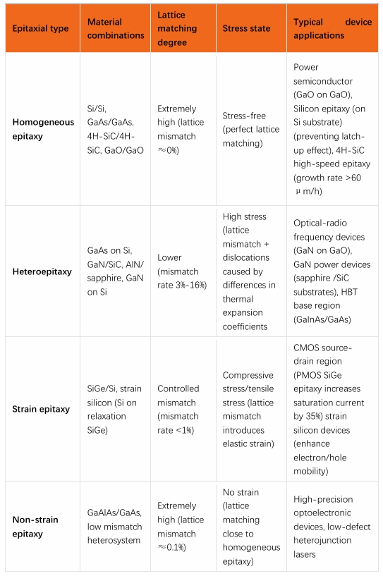
1) Lattice Mismatch and Stress Generation Principles
In heteroepitaxy, the difference in lattice constants between the substrate and the epitaxial layer is the primary cause of stress generation. When the lattice constant of the epitaxial material is larger than that of the substrate (as in the SiGe/Si system), the epitaxial layer experiences compressive stress; conversely, tensile stress is induced. The lattice mismatch rate (Δa/a) can be calculated using the formula:
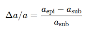
For instance, the lattice mismatch between GaN and sapphire substrates is as high as 16%, which significantly increases the probability of atomic misalignment. To suppress dislocations, techniques such as nano-patterned AlN templates are required. In contrast, homogeneous epitaxy—due to identical materials and perfectly matched lattice constants—enables stress-free, two-dimensional layer growth in the Frank–Van der Merwe mode.
2) Typical Cases of Strain Epitaxy: Performance-Enhancing Mechanisms in SiGe/Si Systems
In the 65/45 nm CMOS process, SiGe strain epitaxy is applied to the source–drain regions of PMOS devices. Leveraging the lattice constant difference between SiGe and Si (the atomic radius of Ge is larger than that of Si), a compressive epitaxial layer is formed on the Si substrate. This compressive stress modifies the valence band structure of Si, reduces the effective hole mass, increases hole mobility by 30%–50%, and ultimately leads to a 35% enhancement in the saturation current (Idsat). Similarly, epitaxial Si grown on a relaxed SiGe layer introduces tensile stress, enhancing electron mobility and further improving device switching speed.
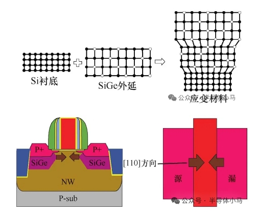
Key Technical Points: Epitaxial growth modes directly determine film quality: layered growth (2D) is typical for lattice-matched systems (e.g., Si/Si), island growth (3D) occurs in highly mismatched systems (e.g., GaN/sapphire), while the Stranski–Krastanov (SK) mode—initial 2D growth followed by 3D islands—is the characteristic pattern of strain epitaxy (e.g., SiGe/Si).
Among the four types of epitaxy, homogeneous epitaxy offers high crystal quality as its core advantage, heteroepitaxy achieves functional expansion through material combinations, and strain epitaxy surpasses carrier mobility limits through stress engineering. Collectively, these techniques drive semiconductor devices toward higher power, higher frequency, and greater integration.
PART03
Growth Mechanisms and Kinetic Controls
The core of semiconductor epitaxial growth lies in the dynamic regulation at the atomic scale, and the process can be systematically described through the "atomic migration - nucleation - growth" three-stage model. The model, in combination with molecular dynamics simulations, reveals the decisive influence of key parameters such as temperature and surface energy on the quality of the thin film, and explains the formation mechanism of the epitaxial layer surface morphology through the evolution patterns of Frank-van der Merwe, Volmer-Webe and Stranski-Krastanov (S-K) models.
1) The Three-Stage Growth Kinetics Model
The atomic-level process of epitaxial growth follows strict temporal logic and can be divided into the following three stages:
Atomic migration stage: The source atoms (such as Ga, N atoms) undergo adsorption, diffusion and desorption behavior on the substrate surface, and the migration length is directly affected by temperature. Molecular dynamics simulations show that temperature regulates the diffusion capacity by altering the thermal motion energy of atoms. When the temperature is too low (for instance, the growth of GaN is below 980 ° C), the insufficient migration energy of atoms leads to a shortened diffusion length, and the atoms that have not fully migrated are prone to form point defect aggregation. Deteriorating X-ray diffraction (XRD) full width at half maximum (FWHM) to over 800 arcsec; High temperatures (such as GaN growth above 1120 ° C) can cause three-dimensional island growth due to high atomic mobility, and the surface roughness (RMS) will sharply increase from 0.2 nm to over 1.5 nm.
Nucleation stage: Atoms migrating to a stable position form an initial structure through two-dimensional (2D) or three-dimensional (3D) nucleation. Two-dimensional nucleation is characterized by the formation of discrete atomic islands on the substrate surface, which gradually merge into continuous two-dimensional layers as atoms continue to adsorb; Three-dimensional nucleation, on the other hand, directly forms isolated three-dimensional islands, which can cause surface undulations. Growth stage: The nucleating structure expands into a single crystal film through methods such as step flow and island merging. For example, in the homoepitaxy of 4H-SiC, the atomic step structure formed by high-temperature in-situ etching (above 1600℃) can guide the growth of the step flow mode and prevent the formation of 3C-SiC heterophy phase. In heteroepitaxy, lattice mismatch or strain accumulation may trigger "layer-island" transitions, such as the strain relaxation process in the S-K mode.
A Core Feature of the Three-Stage Model
Temperature sensitivity: The optimal growth window for GaN is 1000-1100 ° C, and a temperature deviation of ±5 ° C can result in an order of magnitude change in dislocation density. Surface energy drive: For layered growth, the surface energy of the epitaxial layer must be lower than that of the substrate, while for island growth, the opposite is true. The S-K mode is a transitional state between the two.
2) Growth Patterns and Surface Morphology Evolution
The macroscopic morphology of the epitaxial layer is determined by the growth mode, mainly including the following three typical mechanisms, whose transitions are jointly regulated by lattice matching, strain state and process parameters:
1.Layered Growth (Frank-Van Der Merwe Mode)
Atoms grow preferentially in a two-dimensional layered manner when the epitaxial layer has a high lattice fit with the substrate and a low surface energy. For instance, in silicon vapor phase epitaxy, Si atoms grow laterally in two dimensions layer by layer on the substrate surface through a six-step process of "transport - adsorption - reaction - desorption - release - addition", and their morphology is closely related to the "platform - step - torsional position" structure of the crystal face. In this mode, the surface flatness of the epitaxial layer is high, and the RMS can be controlled below 0.5 nm, making it suitable for scenarios with strict interface quality requirements such as high-frequency devices.
2.Island Growth (Volmer-Weber Model)
When the lattice mismatch is large or the surface energy is high, atoms are more likely to form three-dimensional island structures. In the case of heterogeneous epitaxy of GaN on sapphire substrate, when the temperature exceeds 1120 ° C, the surface mobility of Ga atoms is too high, breaking through the two-dimensional nucleating energy barrier and directly forming isolated three-dimensional islands, resulting in a significant increase in surface roughness. Such growth patterns are prone to introducing grain boundaries and dislocations, and the overgrowth of three-dimensional islands needs to be suppressed through temperature field simulation optimization (such as PID temperature control technology).
3.Stranski-Krastanov (S-K) Mode
This pattern is a transitional form from layered to island-like and is commonly found in strain epitaxial systems. In the initial stage, the epitaxial layers grow in two-dimensional layers (typically 1-3 atomic layers), and when the strain accumulation exceeds the critical value (such as the strain threshold of AlN on a sapphire substrate), the system releases the strain by forming three-dimensional islands to complete the "layer-island" transition. This process is accompanied by the generation of dislocations and other defect. The lateral epitaxial direction can be regulated by techniques such as "nano-patterned AlN template" (NPAT) to suppress the dislocation density to the order of ~10⁴ cm⁻².
Dynamic control of the above-mentioned growth patterns is a core challenge in the epitaxy process. Precise control over the entire process of "atomic migration - nucleation - growth" can be achieved by optimizing temperature gradients (such as a 50% increase in dislocation density for every 1 ° C /mm increase in GaN MOCVD), gas flow field distribution (regional division intake regulation for uniform transport), and substrate surface pretreatment (such as in-situ etching of 4H-SiC to form atomic steps) Lay the material foundation for high-performance semiconductor devices.
