Paper Sharing
【Member Papers】Sn-assisted epitaxial growth of high-crystallinity κ/ε-Ga₂O₃ on sapphire (0001) by low-pressure Mist-CVD
日期:2025-10-16阅读:590
Researchers from the Hong Kong University of Science and Technology (Guangzhou), have published a dissertation titled "Sn-assisted epitaxial growth of high-crystallinity κ/ε-Ga2O3 on sapphire (0001) by low-pressure Mist-CVD" in Applied Physics Letters.
Project Support
The work was supported by C. K. Tan start-up fund from the Hong Kong University of Science and Technology (Guangzhou); the Guangzhou Municipal Science and Technology, Project Nos. 2023A03J0003, 2023A03J0013, 2023A04J0310, and 2023A03J0152; the Department of Education of Guangdong Province, No. 2024ZDZX1005; the State Administration of Foreign Experts Affairs (No. Y20240005); and the Characterization and Preparation Facility (MCPF) and Green e Materials Laboratory at The Hong Kong University of Science and Technology (Guangzhou).
Background
Gallium oxide (Ga2O3) has emerged as a key material for power electronics due to its ultra-high breakdown field, excellent Baliga’s figure of merit, and strong radiation tolerance. Traditionally, the β phase has dominated high-voltage device applications because of its proven stability and commercial viability. Recently, attention has shifted to the metastable ε phase (ε-Ga2O3), which combines high spontaneous polarization (~25 μC/cm2) with a large piezoelectric coefficient (d₃₃ ≈ 10.8–11.2 pm/V), making it a promising candidate for next-generation high-electron-mobility transistors (HEMTs) and radio-frequency resonators.
The epitaxial growth of high-quality ε-Ga2O3 films remains a critical challenge. Tin (Sn) doping has been shown to stabilize the ε phase by suppressing competing β/α phases and improving surface morphology, thereby enhancing the thermal stability of the metastable phase. However, device-grade films require precise control over crystallinity, interfacial abruptness, and thickness uniformity—requirements that current growth techniques struggle to satisfy.
Mist chemical vapor deposition (Mist-CVD) offers a cost-effective approach for ε-Ga2O3 epitaxy but suffers from limited process optimization and broad rocking curve widths. Alternative techniques such as MOCVD, HVPE, and ALD show some improvements in crystal quality but face trade-offs in cost, thickness control, or processing conditions.
Consequently, achieving high-quality ε-Ga2O3 films that simultaneously meet the demands of cost, crystallinity, and process control remains a central challenge for advancing power and high-frequency electronic devices.
Abstract
The ultrawide-bandgap gallium oxide (Ga2O3) polymorphs have opened frontiers in high-power electronics and multifunctional devices. Among these, the orthorhombic phase (commonly referred to as κ-Ga2O3 or ε-Ga2O3, hereafter denoted as ε-Ga2O3 in this work) stands out with its exceptional spontaneous polarization and large piezoelectric coefficients, positioning it as a prime candidate for next-generation high-electron mobility transistors and radio frequency resonators. However, the epitaxial growth of high-quality ε-Ga2O3 films remains challenging due to interfacial transition layers and limited crystallographic control. Herein, we demonstrate a pioneering Sn-assisted low-pressure mist chemical vapor deposition technique that enables the growth of single-phase ε-Ga2O3 films on c-plane sapphire substrates with unprecedented crystalline quality. The resulting films exhibit a remarkably narrow x-ray diffraction rocking curve (full width at half maximum, FWHM = 0.08°) while achieving atomically smooth surfaces (root mean square, RMS roughness = 1.51 nm). Key innovations include the complete suppression of interfacial transition layers through Sn-mediated nucleation and the realization of true layer-by-layer growth under optimized low-pressure conditions. This synergistic approach combines the inherent cost-effectiveness of Mist-CVD with enhanced crystallographic precision, establishing a viable pathway for industrial-scale production of ε-Ga2O3-based quantum well devices and polarization-engineered heterostructures.
Conclusion
The Sn-assisted LP-Mist-CVD technique represents a groundbreaking leap in ε-Ga2O3 epitaxy, uniquely addressing the long-standing challenges of interfacial phase suppression and crystallographic precision through its synergistic integration of Sn-mediated nucleation and low-pressure process optimization. By enabling true layer-by-layer growth with atomically smooth surfaces (RMS¼1.51nm) and high e-phase quality (XRD FWHM¼0.08 ), this method outperforms conventional Mist-CVD and rivals high-cost HVPE while maintaining cost efficiency and thickness controllability. The elimination of parasitic α-Ga2O3 phases and unprecedented interfacial abruptness establish a transformative plat form for advanced oxide electronics, particularly in polarization engineered heterostructures and HEMTs. Demonstrating compatibility with sapphire substrates and low precursor consumption, LP Mist-CVD not only redefines the growth paradigm for ε-Ga2O3 but also unlocks scalable fabrication of ultrawide-bandgap devices demanding atomic-level interface control, positioning it as an industrially viable solution for next-generation power and quantum electronics.
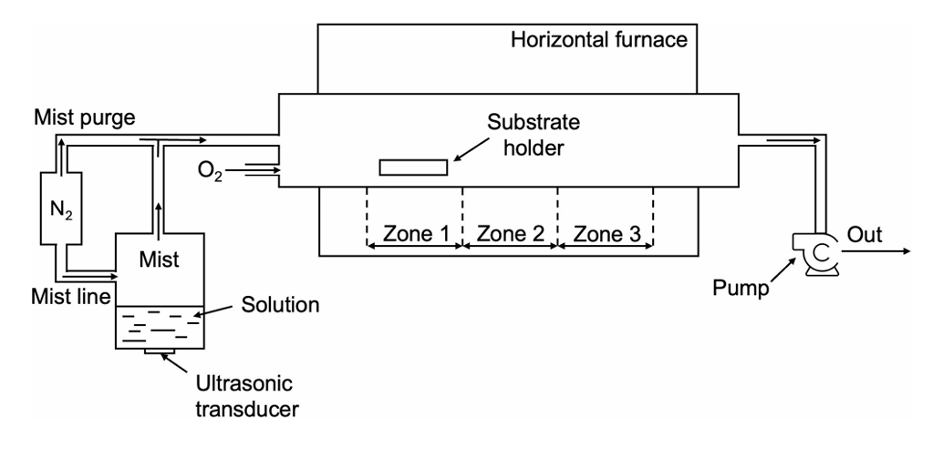
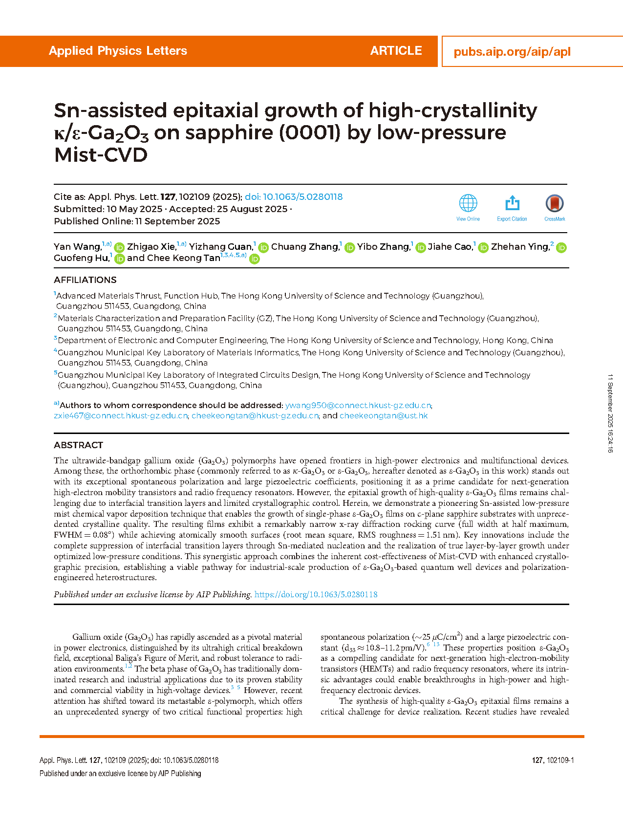
FIG. 1. Illustration of the low pressure Mist-CVD (LP-Mist-CVD) system.
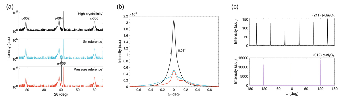
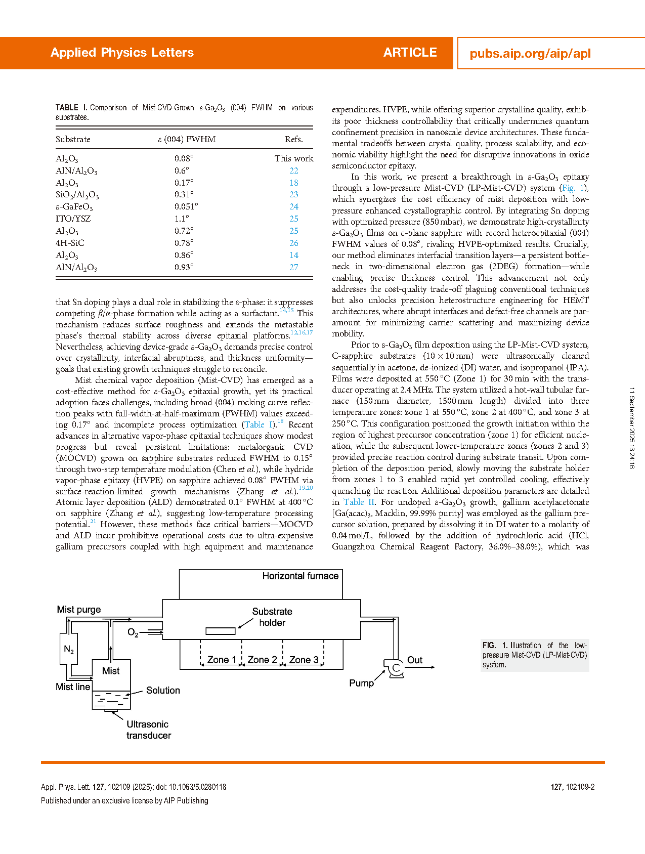
FIG. 2. (a) XRD 2h-scan profiles of all three samples. (b) XRD rocking curves of the ε-Ga2O3 (004) reflection for the three samples, measured under identical conditions. (c) XRD u-scan of the high-crystallinity sample for the (211) plane of ε-Ga2O3 and the (012) plane of α-Al2O3.
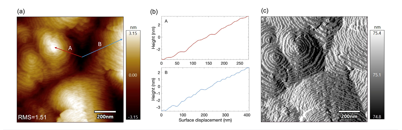
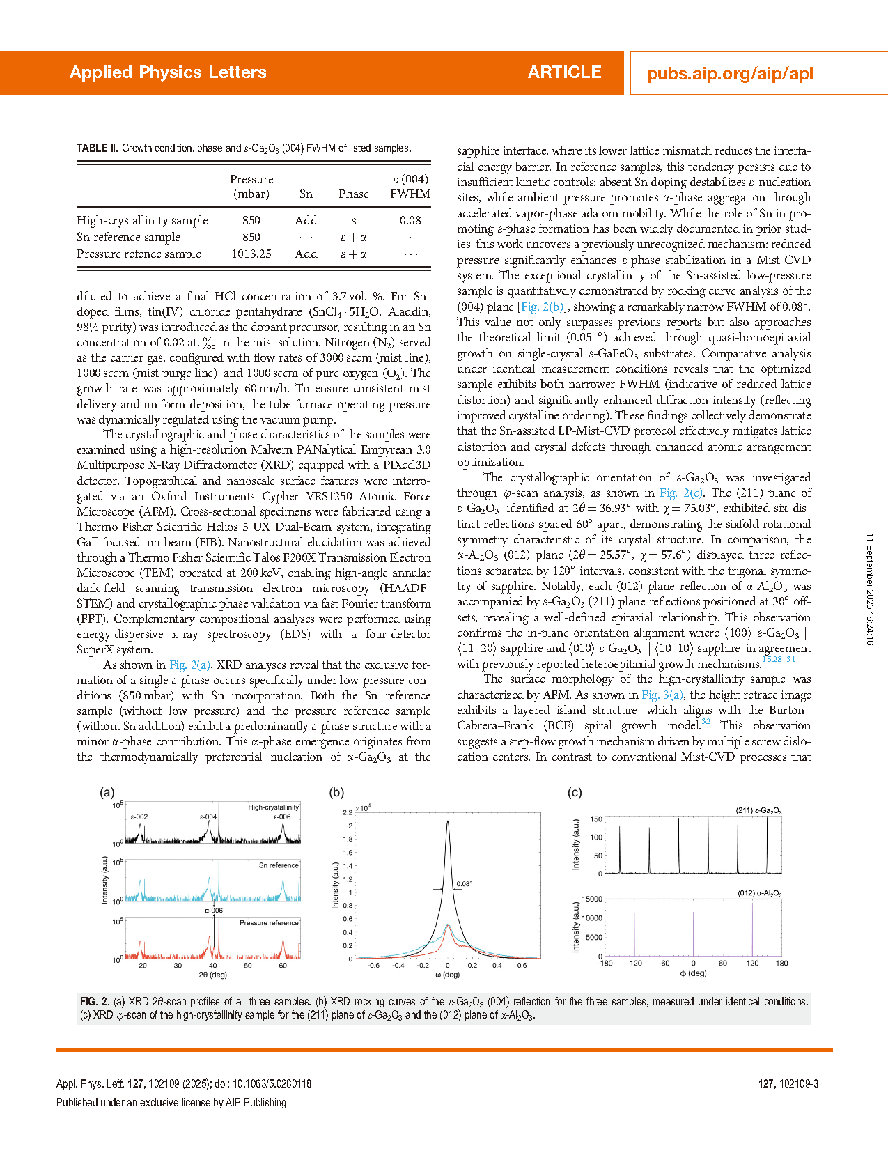
FIG. 3. AFM images of the high-crystallinity sample surface. (a) Height retrace image. (b) Height profiles measured along directions A and B. (c) Amplitude retrace image.

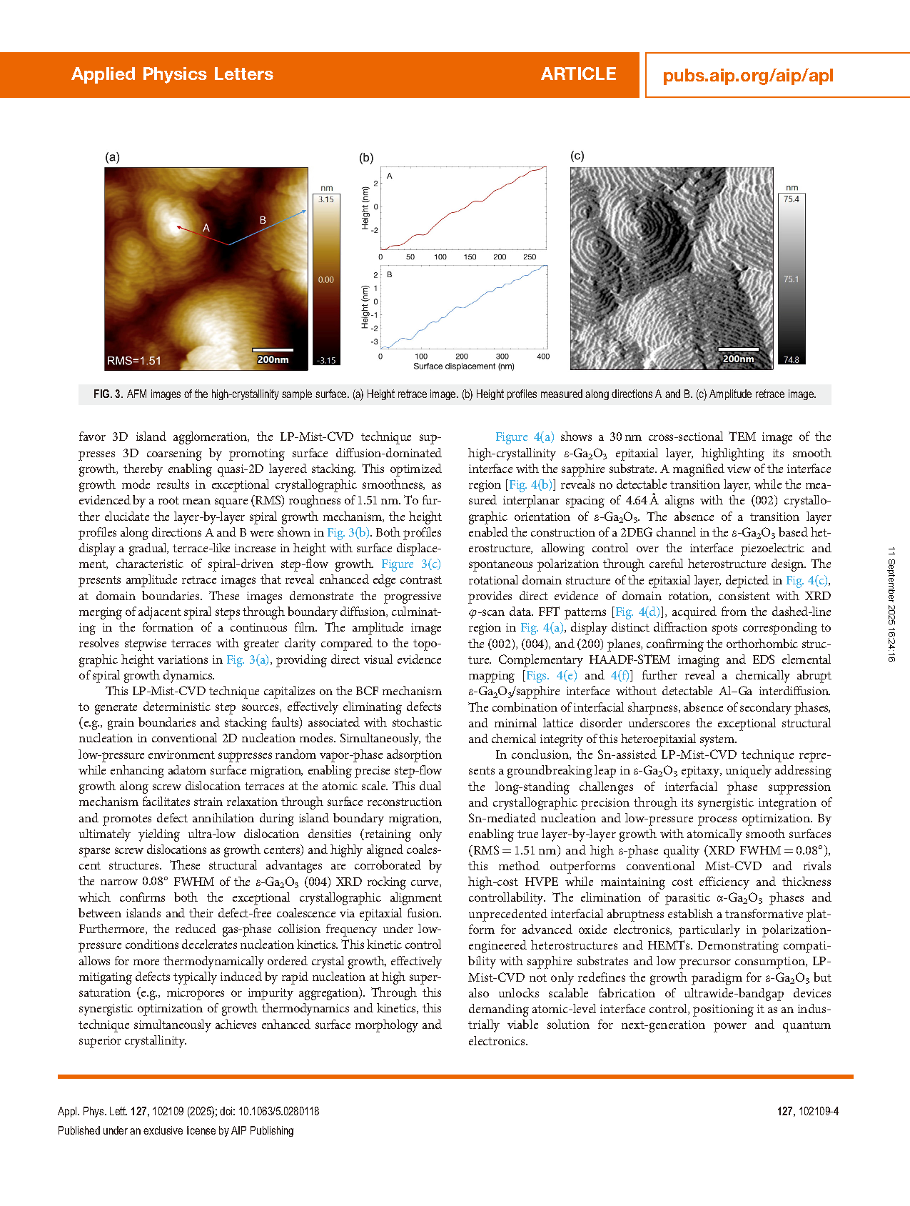
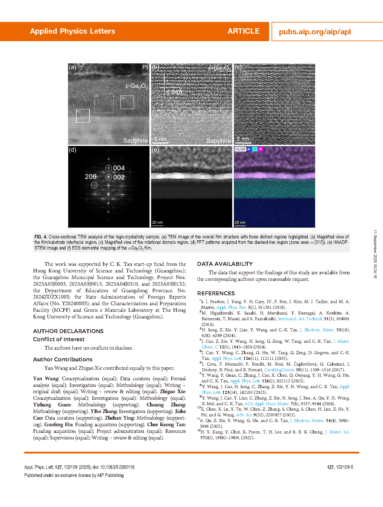
FIG. 4. Cross-sectional TEM analysis of the high-crystallinity sample. (a) TEM image of the overall film structure with three distinct regions highlighted. (b) Magnified view of the film/substrate interfacial region. (c) Magnified view of the rotational domain region. (d) FFT patterns acquired from the dashed-line region (zone axes¼ [010]). (e) HAADF STEM image and (f) EDS elemental mapping of the ε-Ga2O3 film.
DOI:
doi.org/10.1063/5.0280118