


Paper Sharing
【Member Papers】Full-space built-in electric field inside gradient Sn-doped β-Ga₂O₃ photoanodes for enhanced photoelectrochemical solar-blind UV photodetection
日期:2025-10-17阅读:630
Researchers from the Chongqing Normal University have published a dissertation titled "Full-space built-in electric field inside gradient Sn-doped β-Ga₂O₃ photoanodes for enhanced photoelectrochemical solar-blind UV photodetection" in Science China Materials.
Abstract
β-Ga2O3 is a promising candidate for solar-blind ultraviolet photodetection owing to its suitable bandgap of approximately 4.9 eV, excellent photoresponse characteristics, and high stability. However, lack of a sufficient driving force within the material leads to extensive bulk charge recombination, limiting its photocurrent and thus posing significant challenges in designing high-performance Ga2O3-based photodetection. In this study, we propose a gradient doping strategy to achieve a Sn-doping concentration gradient along the β-Ga2O3 film thickness. By combining sol–gel synthesis with rapid thermal annealing, a spatially graded band structure with a full-space built-in electric field is constructed, which increases the width of band bending over a large region and is crucial for significantly enhancing carrier separation and transport in the bulk. The resulting gradient Sn-doped β-Ga2O3 enables exceptional photoelectric performance without an external bias under 254 nm irradiation, including a superior responsivity of 66.88 mA/W, a high detectivity of 8.12×10¹¹ Jones, and a fast rise/decay time of 79/65 ms, outstanding most existing similar reported photoelectrochemical-type optoelectronic devices. Additionally, the device exhibits excellent long-term stability and enables high-resolution underwater ultraviolet imaging. This study demonstrates that the gradient doping strategy provides a feasible approach for enhancing the photoelectrochemical performance of β-Ga2O3 photoelectrodes.
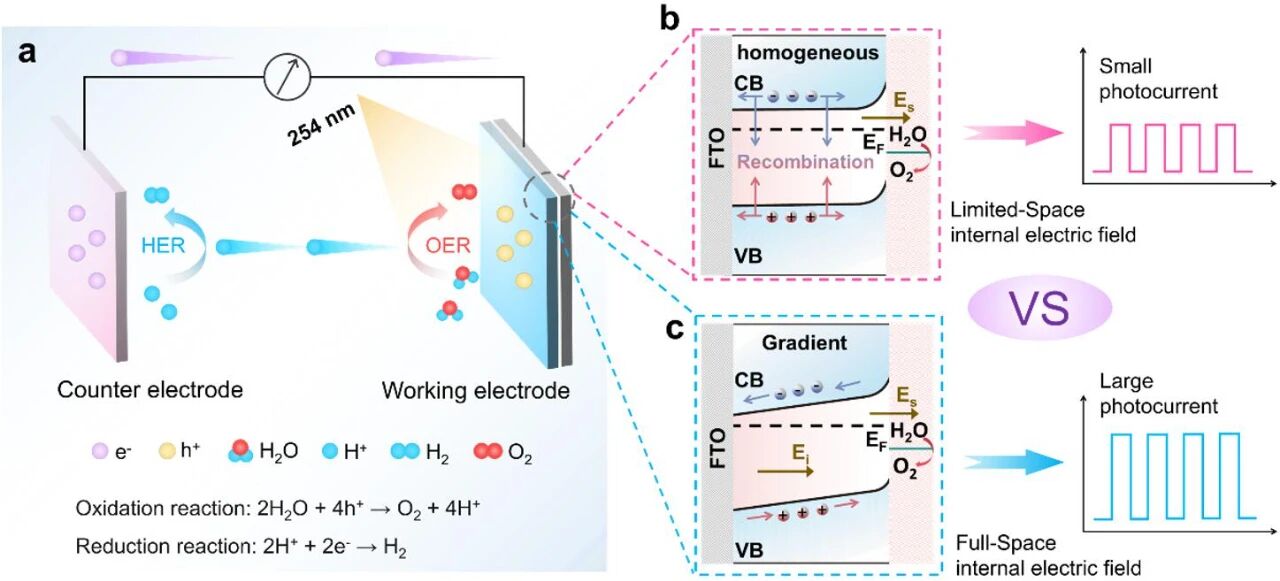
Figure 1. Energy band diagrams. (a) Schematic illustration of the PEC-type photodetector. Band bending schematics and the resulting photocurrents of (b) homogeneous doped photoanode and (c) gradient-doped photoanode. CB, conduction band; VB, valence band; EF, Fermi level; Ei, electric field arising from the gradient doping; Es, electric field arising from the β-Ga2O3/electrolyte junction.
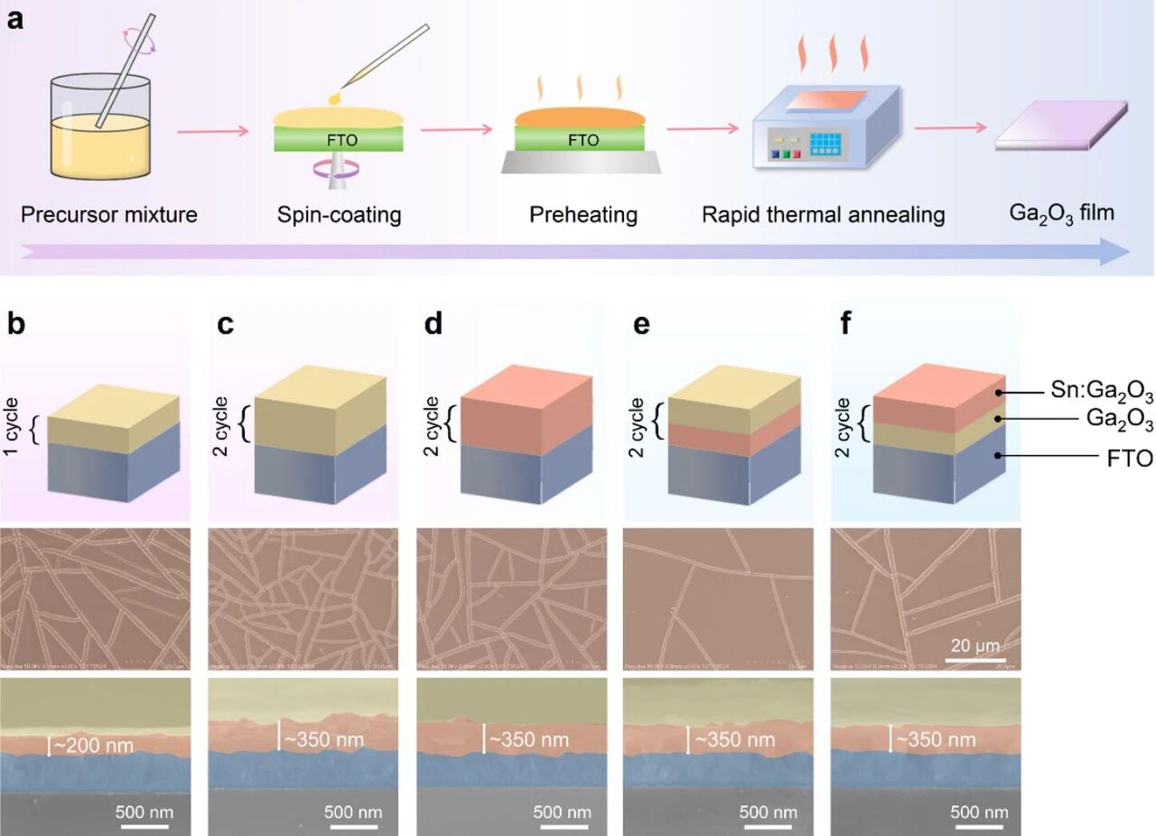
Figure 2. Schematic diagrams of Sn-doped Ga2O3 films. (a) Fabrication process of β-Ga2O3 films via sol-gel method. Schematic of the β-Ga2O3 films prepared with (b) one cycle, (c) two cycles, (d) homogeneous, (e) gradient, and (f) reverse gradient Sn doping; the corresponding SEM images are also included.
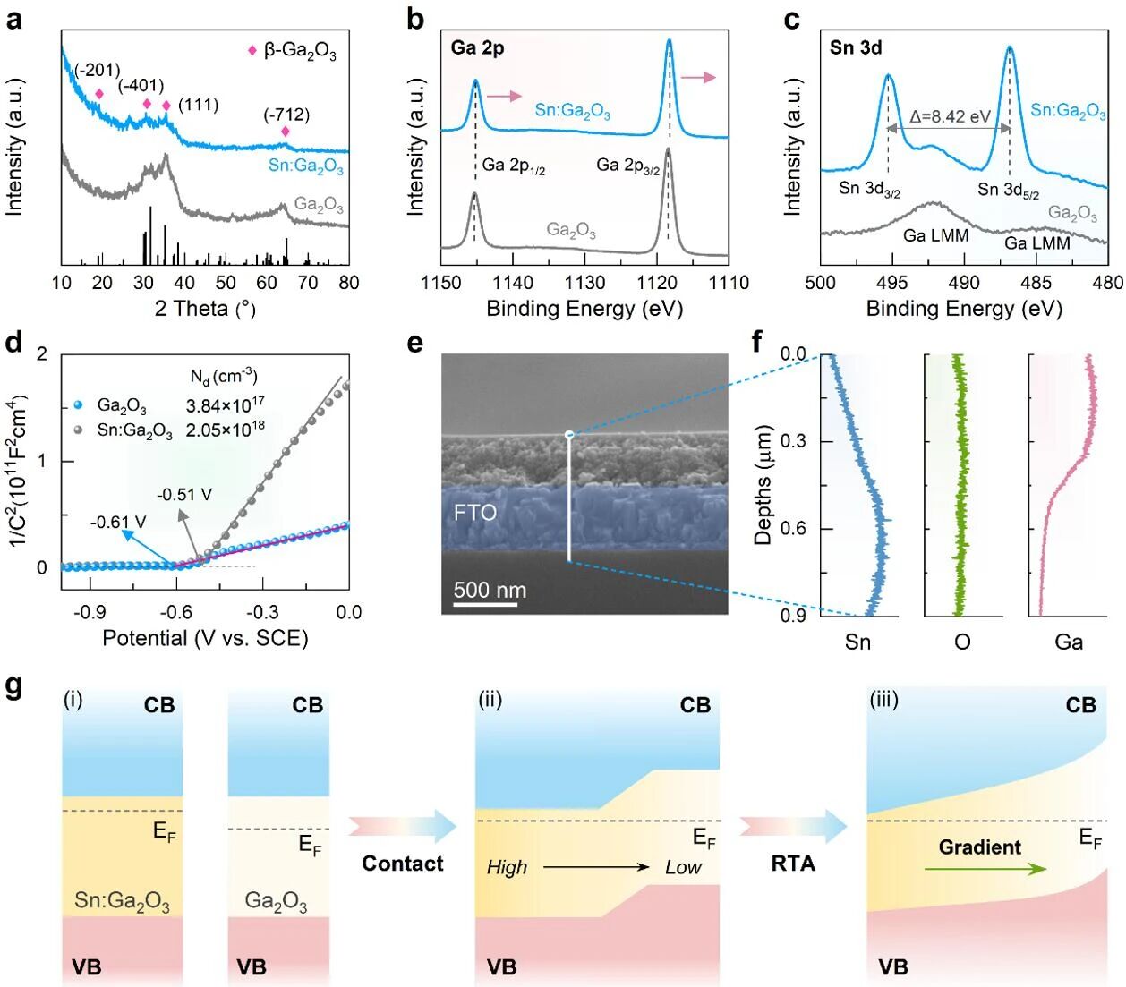
Figure 3. Material characterizations. (a) GIXRD patterns, (b) Ga 2p core-level XPS spectra, (c) Sn 3d core-level XPS spectra, and (d) Mott-Schottky curves of the Ga2O3 film and the Sn:Ga2O3 film with a Sn content of 6%. (e) Cross-sectional SEM image and (f) EDS linear scan profile of the gradient Sn:Ga2O3 film. (g) Schematic band alignments of gradient Sn:Ga2O3 film before contact (i), after contact (ii), and the formed full-space electric field after rapid thermal annealing (iii).
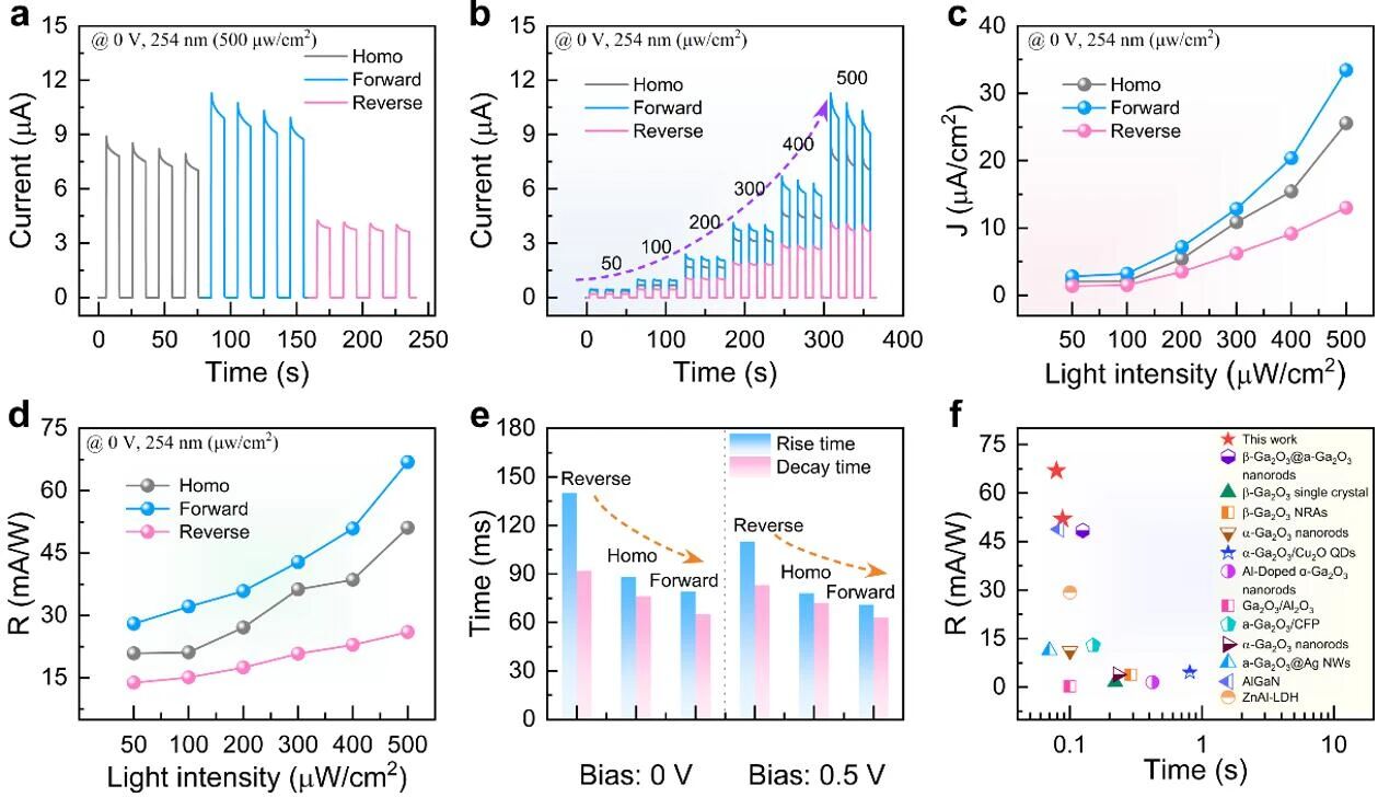
Figure 4. Evaluation of self-powered PEC performance. (a) I-t curves of homogeneous, gradient, and reverse gradient Sn:Ga2O3 films under 254 nm (500 μW/cm2) illumination and 0 V bias in 0.5 M Na2SO4. (b) I-t curves and (c) corresponding photocurrent density under various light intensities. (d) Calculated responsivity values as a function of incident light intensities. (e) Response time under 0 V and 0.5 V. (f) Performance comparisons of PEC-type UV photodetectors in this work and other reported device.
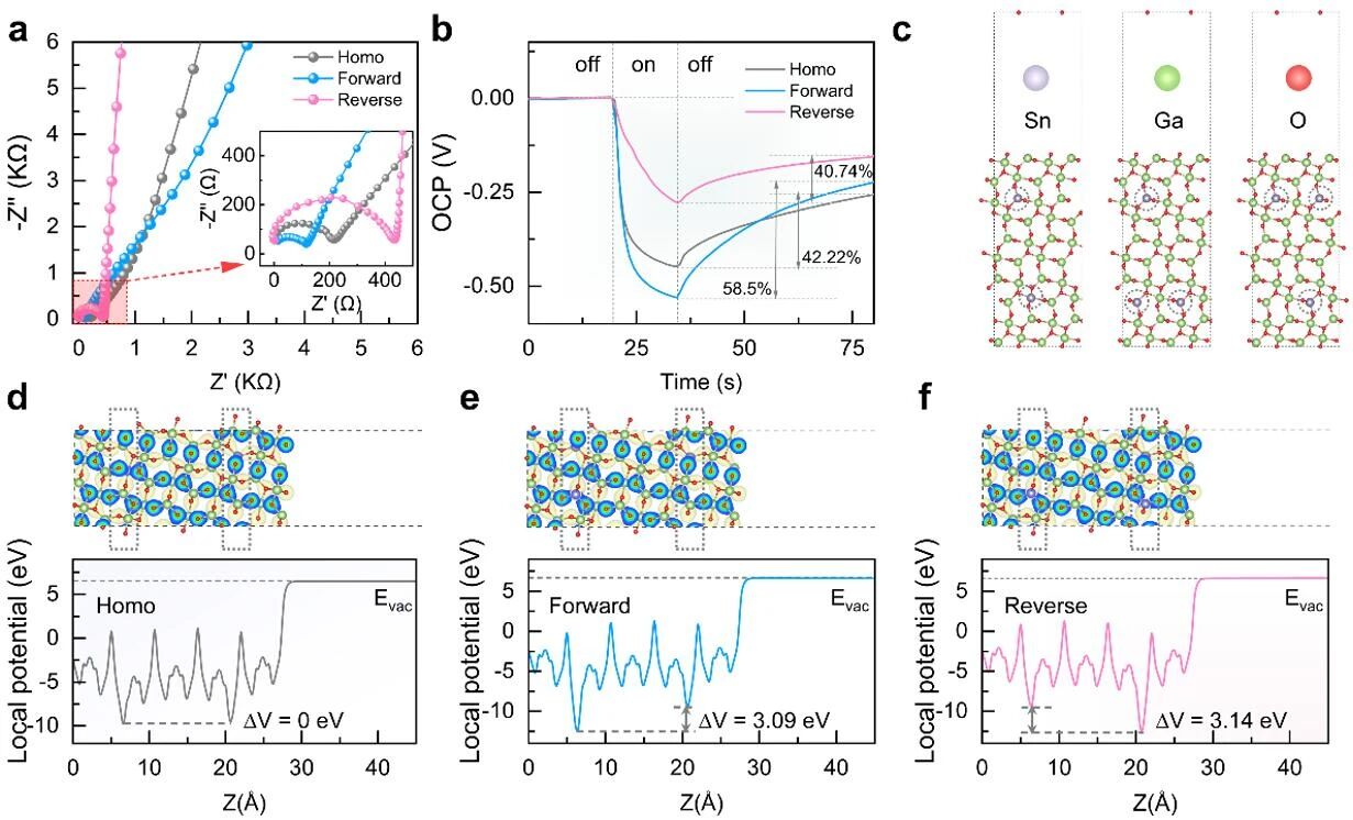
Figure 5. Characterization of charge carrier dynamic and electronic structure properties. (a) EIS profiles of homogeneous, gradient, and reverse gradient Sn:Ga2O3 photoanodes; the inset shows the enlarged view of the high-frequency region in EIS profiles. (b) Open circuit potential (OCP) plots. (c) Optimized structure of β-Ga2O3 photoanode with (left) homogeneous, (middle) gradient, and (right) reverse gradient Sn doping. (d–f) 3D charge density difference and plane-averaged electrostatic potential drop across the interface for (d) homogeneous, (e) gradient, and (f) reverse gradient Sn:Ga2O3 photoanodes. Evac represent the vacuum level.
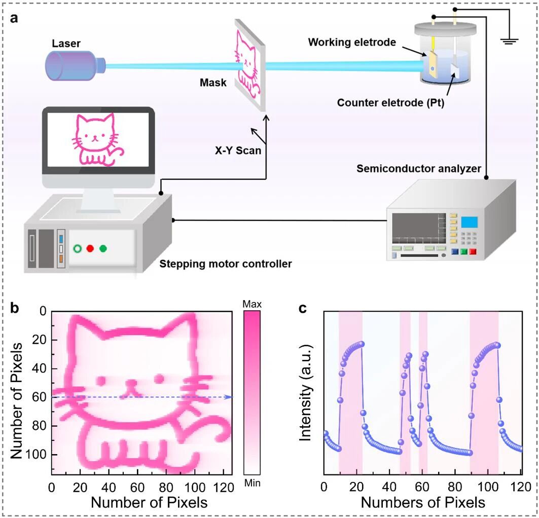
Figure 6. Schematic representation of the device application. (a) Schematic diagram of the underwater optical imaging system. (b) Image obtained from the image scanning system. (c) Cross section of continuous current value at straight line position in (b).
论文信息:
Ke Zhai, Hong Zhang*, Shiyi Li, Jieneng Chen, Pukai Zhou, Hang Cui, Di Pang, Yan Tang, Lijuan Ye, Honglin Li* and Wanjun Li*. Full-space built-in electric field inside gradient Sn-doped β-Ga2O3 photoanodes for enhanced photoelectrochemical solar-blind UV photodetection. Science China Materials, 2025, DOI: 10.1007/s40843-025-3757-2.
论文链接:
https://doi.org/10.1007/s40843-025-3757-2
