Paper Sharing
【Member Papers】Effect of Atomic-Level Roughness on Vertical β-Ga₂O₃ Schottky Barrier Diode and High-Temperature Performance
日期:2025-10-17阅读:547
Researchers from the Shenzhen Pinghu Laboratory have published a dissertation titled "Effect of Atomic-Level Roughness on Vertical β-Ga2O3 Schottky Barrier Diode and High-Temperature Performance" in 2025 IEEE Workshop on Wide Bandgap Power Devices and Applications in Asia (WiPDA Asia).
Project Support
This work is supported by the Shenzhen Pinghu Laboratory Project (Grant No. 224110).
Background
β-phase Ga2O3 has emerged as a highly promising ultra-wide bandgap semiconductor (∼4.8 eV) for next-generation power electronics, exhibiting superior material characteristics, enabling revolutionary performance in high-voltage rectifiers, power conversion systems, and extreme-environment electronic devices. β-Ga2O3 Schottky barrier diode (SBD) as rectifier ensures robust operation at high-temperature and in harsh environment. Moreover, the compatibility of Ga2O3 with cost-effective melt-growth technique further enhances its scalability for power electronics.
The air-exposed surface of β-Ga2O3 epi-wafers may contain impurities and contaminations, such as adsorbed carbon, surface voids, and native oxides. Interface states and defects may account for conduction and blocking properties in Ga2O3 power devices. The high-quality interface is critical to device performance. Therefore, surface pre-treatments are needed to optimize the surface roughness and quality. The roughness of the Ga2O3 surface is also the key aspect for Schottky barrier height (SBH) homogeneity. In recent years, numerous surface treatment strategies for β-Ga2O3 Schottky diodes, such as annealing, wet chemical, F-plasma and dry etching, have been used to enhance the interface quality and reduce roughness. Among them, inductively coupled plasma (ICP) etching can effectively improve the surface quality. However, atomic-scale surface roughness of β-Ga2O3 wafer is still a challenge.
Abstract
We demonstrate the atomic scale surface roughness of β-Ga2O3 epitaxial layer by developing a two-step inductively coupled plasma and wet-repair treatment. The superior surface roughness of 0.12 nm and close-to-unity ideal factor (n) of 1.05 were achieved using optimized surface treatment on vertical β-Ga2O3 Schottky barrier diodes (SBDs). Compared to untreated samples, the blocking capability was enhanced with increasing breakdown voltage (BV) above 1.6 times. Furthermore, a comprehensive analysis of the electrical properties at high temperature was analyzed to verify that the improved Ni/β-Ga2O3 interface quality can lead to an enhancement of the device performance. When subjected to an off-state stress of -100 V at 175, the surface-treated SBDs perform stable forward characteristics with slight current-density degradation (∆Jmax<0.01%). The results pave the way for further improving the surface quality of β-Ga2O3 devices and validate the potential of SBDs in high-temperature power application scenarios.
Conclusion
In summary, we have achieved a smooth surface with a roughness of 0.12 nm by developing the two-step ICP etching and wet-repair surface treatment. Enhanced surface quality can significantly improve the BV above 1.6 times of SBDs. In addition, the ideal factor (n=1.05) was obtained, which was attributed to the low surface density. Off-state stress measurements reveal reliable dynamic performance of surface-treated SBDs under harsh high-temperature conditions.
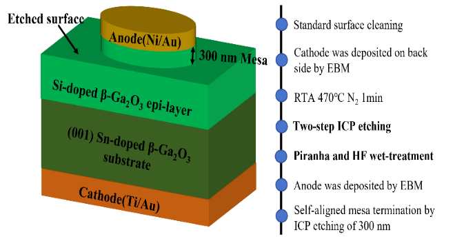
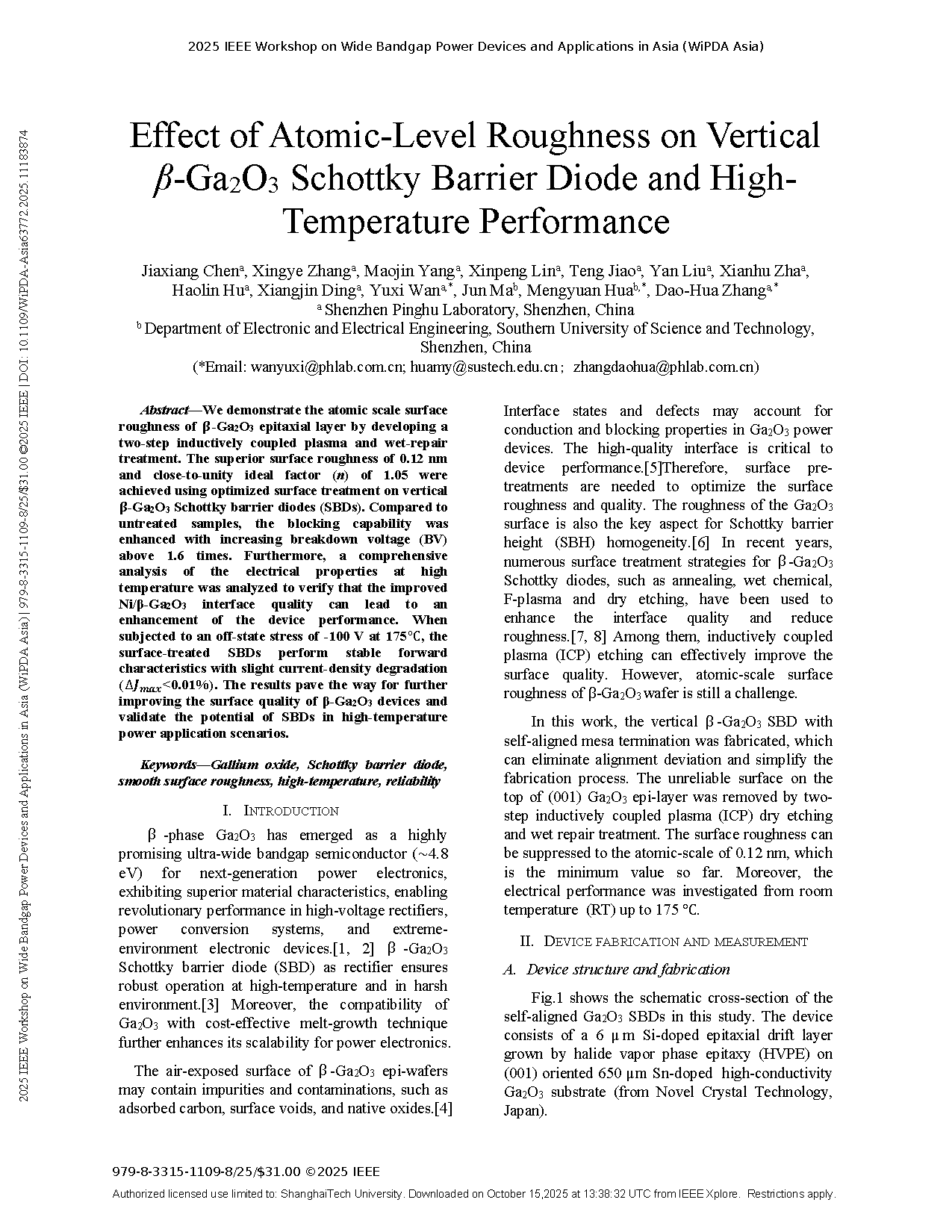
Fig. 1. Schematic cross-sectional structure and main process flow of the self-aligned SBDs used in this work.
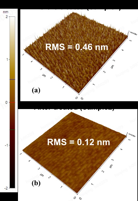
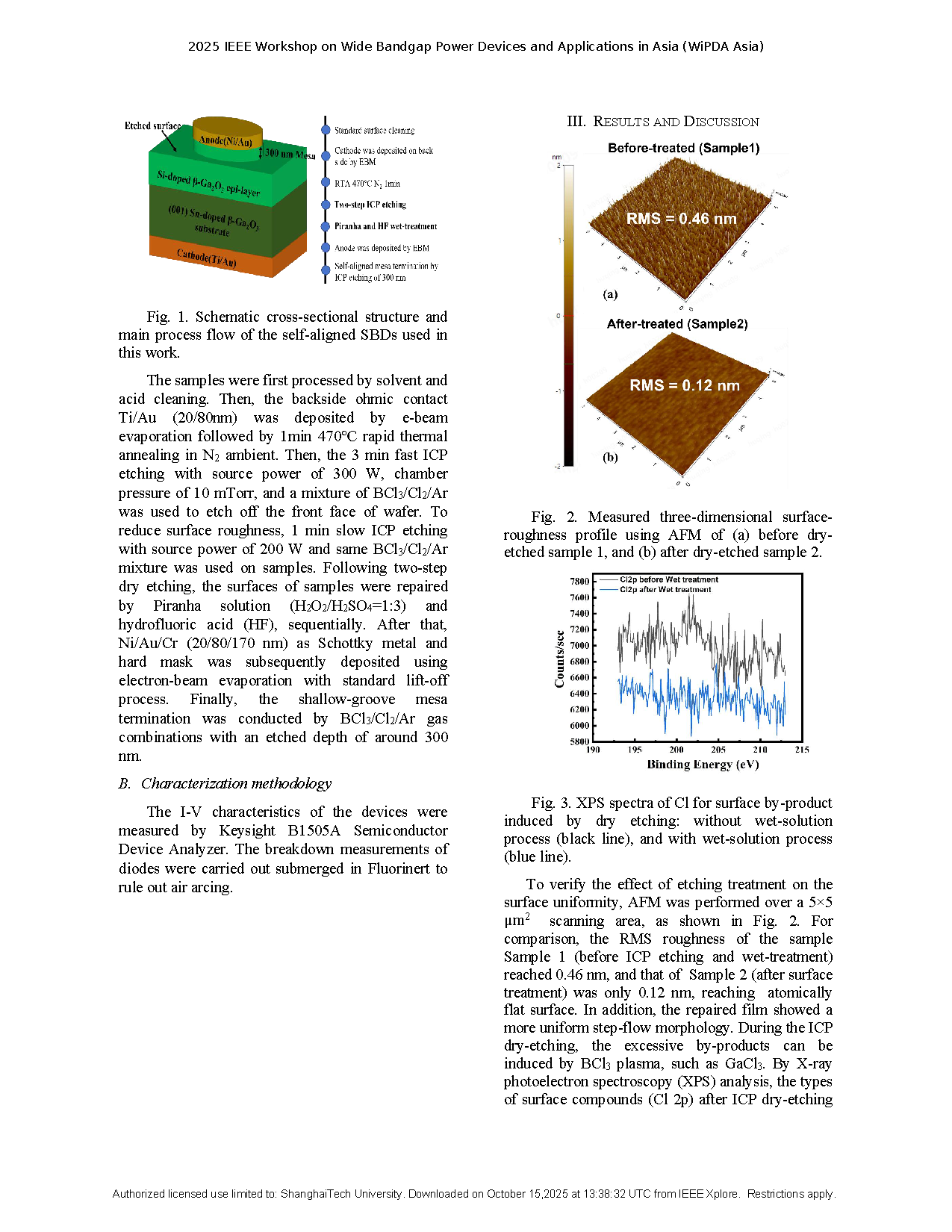
Fig. 2. Measured three-dimensional surface-roughness profile using AFM of (a) before dry-etched sample 1, and (b) after dry-etched sample 2.
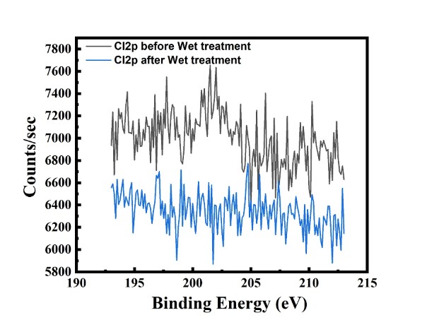
Fig. 3. XPS spectra of Cl for surface by-product induced by dry etching: without wet-solution process (black line), and with wet-solution process (blue line).

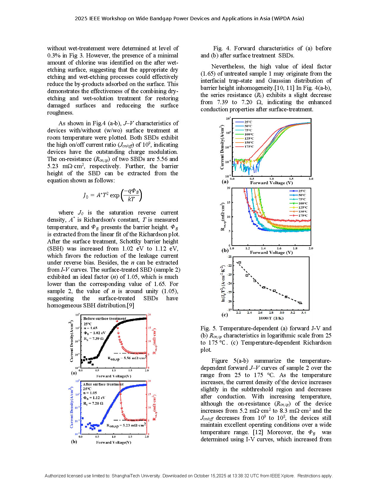
Fig. 4. Forward characteristics of (a) before and (b) after surface treatment SBDs.
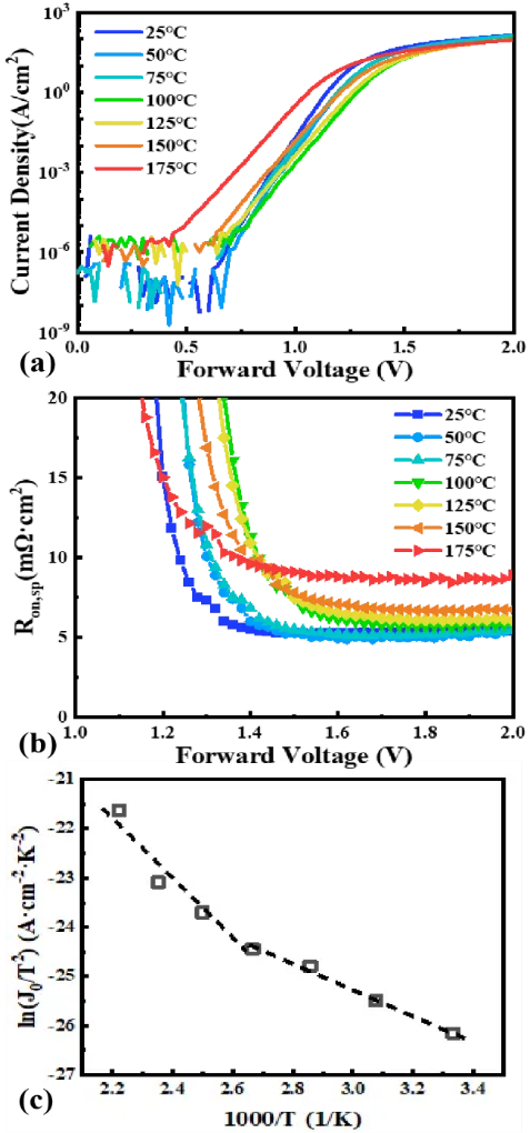
Fig. 5. Temperature-dependent (a) forward J-V and (b) Ron,sp characteristics in logarithmic scale from 25 to 175. (c) Temperature-dependent Richardson plot.
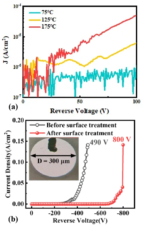
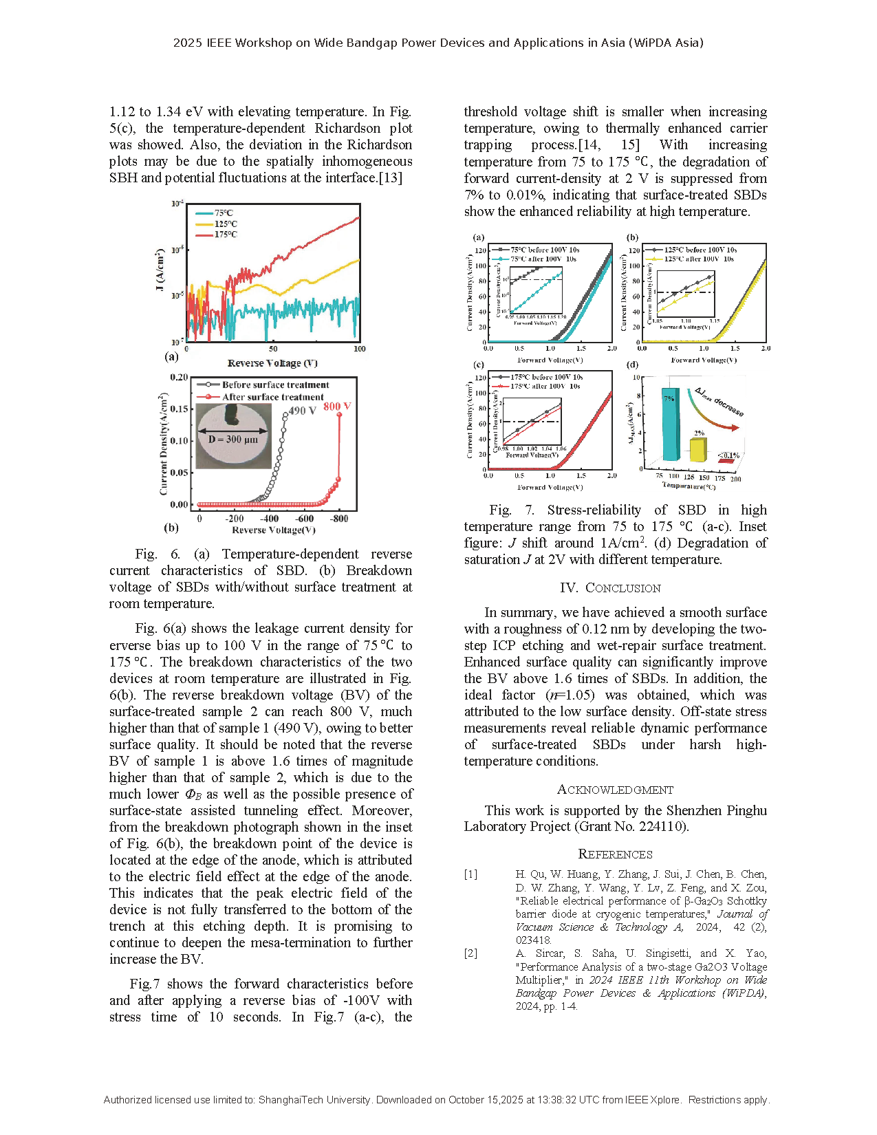
Fig. 6. (a) Temperature-dependent reverse current characteristics of SBD. (b) Breakdown voltage of SBDs with/without surface treatment at room temperature.
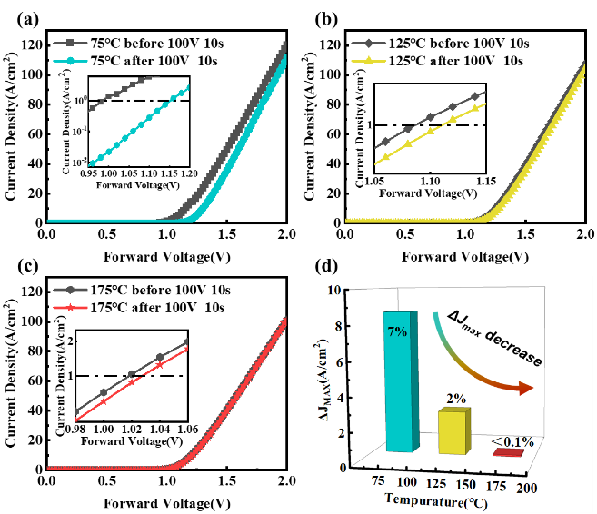
Fig. 7. Stress-reliability of SBD in high temperature range from 75 to 175 (a-c). Inset figure: J shift around 1A/cm2. (d) Degradation of saturation J at 2V with different temperature.
DOI:
https://doi.org/10.1109/WiPDA-Asia63772.2025.11183874