


Member News
【Member News】Shenzhen Pinghu Laboratory — National Center of Technology Innovation for Wide Bandgap Semiconductor (Shenzhen) Unveils Multiple Technology Achievements and Service Platforms
日期:2025-10-20阅读:731
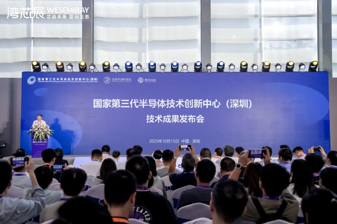
On October 15th, the 2025 Semibay Semiconductor Ecosystem Expo opened at the Shenzhen Convention and Exhibition Center (Futian). The Shenzhen Comprehensive Platform of the National Center of Technology Innovation for Wide Bandgap Semiconductor Shenzhen Comprehensive Platform(referred to as "Shenzhen Comprehensive Platform"), based on the Shenzhen Pinghu Laboratory, showcased a number of core technological achievements and future cutting-edge exploration technologies at the Compound Semiconductor Industry Development Summit Forum. At this industry event that gathered over 600 leading global semiconductor enterprises, With an "open and shared" attitude, it unleashes technological innovation vitality and injects core momentum to address industry pain points.
01 Platform Technology Achievements Release: Highlights Abound, Driving Innovation Forward
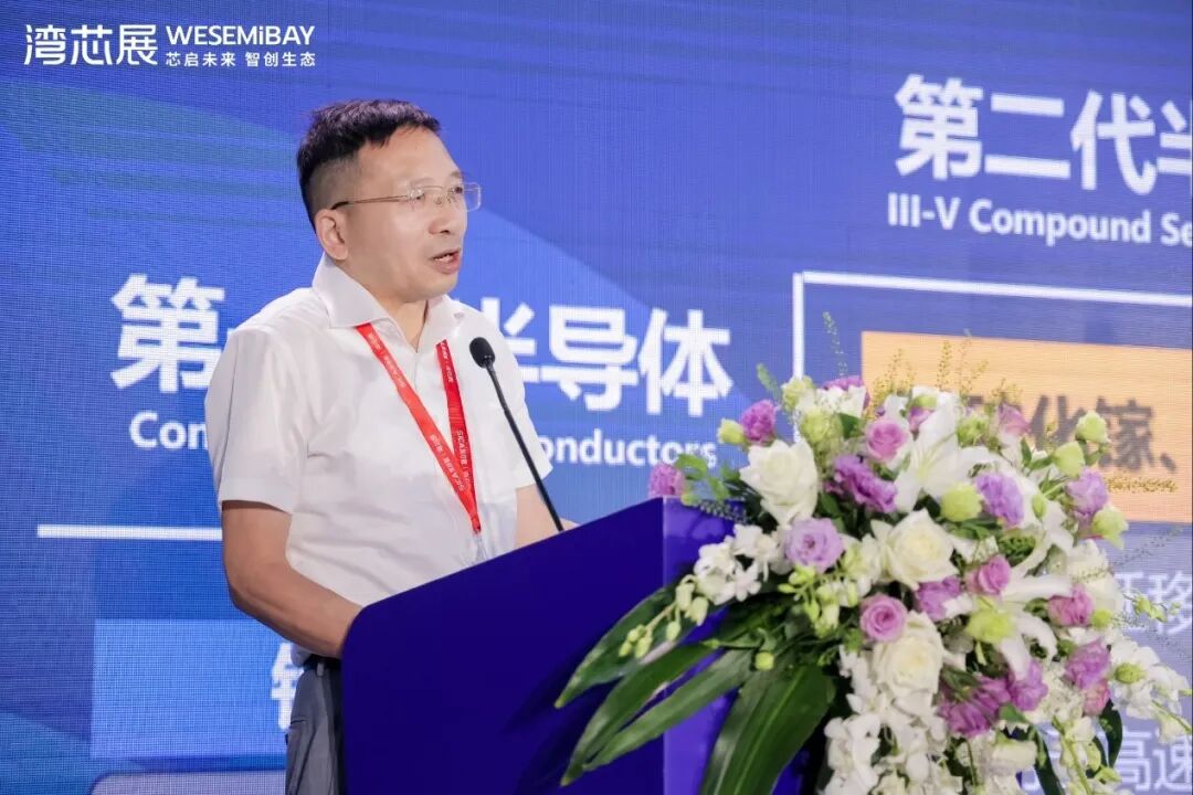
Power semiconductors are high-potential materials for modern power electronic and RF devices, holding equal importance to integrated circuits. Their core competitiveness lies in the seamless integration of materials and device structures, making them particularly suitable for high-voltage, high-frequency, and high-power applications. The third-generation semiconductors, represented by SiC and GaN, as well as the fourth-generation semiconductors, including gallium oxide, aluminum nitride, and diamond, all exhibit vast potential for future applications.
The Shenzhen Integrated Platform is the world’s first open and shared 8-inch advanced power semiconductor platform that integrates scientific research with pilot-scale production, possessing a complete capability chain from R&D to industrialization. The platform comprises four major centers — the Research Center, Pilot Center, Analysis and Testing Center, and Technology Transfer Center. To date, it has served over 30 partners, more than 10 pilot-scale customers, and over 45 clients in analysis and testing services, while establishing research collaborations or joint internship bases with eight universities.
In 2025, the platform successfully launched Technology Platform 1.0, achieving significant breakthroughs in substrate and epitaxial technologies, SiC planar and trench gate processes, and GaN epitaxy and device fabrication.
Substrate Processing Technology:The platform has taken the lead in achieving breakthroughs in silicon carbide laser lift-off (LLO) technology and efficiency, realizing a total wafer loss of less than 75 μm on 8-inch wafers, cutting time within 20 minutes, and a 26% cost reduction. After verification through epitaxy, device fabrication, and reliability testing, the overall performance has reached an internationally leading level. This advancement supports the semiconductor supply chain in achieving higher quality, lower cost, and improved efficiency.
Silicon Carbide Epitaxial Technology:Targeting national strategic applications such as smart grids and rail transit, the platform has advanced research on ultra-high-voltage thick films and super-junction epitaxy. It has successfully tackled key challenges in defect control and minority carrier lifetime enhancement for 200 μm ultra-thick films, reaching internationally advanced standards. For the first time, high-quality 3C-SiC epitaxy has been realized on commercial 4° off-axis 4H-SiC substrates, offering a potential solution to the low gate-oxide mobility problem in SiC power devices.
1200V SiC Planar Gate Technology:Breakthroughs have been achieved in key technologies such as ultra-narrow planar cell structure design and the fabrication of ultra-high aspect ratio source contact holes, establishing strong technical capabilities for high-performance SiC planar-gate MOSFET devices.
1200V SiC Trench Gate Technology:Significant progress has been made in structural precision and damage control, interface quality and reliability, electrical performance optimization, and terminal protection design. The devices now perform at an industry-leading level, backed by fully independent structural patents. A complete, self-controlled 8-inch trench-gate SiC MOSFET process platform has also been established.
GaN Epitaxial Technology:For high-voltage and automotive-grade applications, the platform has conducted 1200V epitaxial research achieving internationally advanced results in GaN-on-Si epitaxial thickness, wafer bow, and vertical breakdown voltage. For low-voltage applications — particularly AI power supply systems in the 15–40V range — the platform has achieved breakthroughs in high-quality selective secondary epitaxy, removing technical bottlenecks for ultra-low-voltage GaN industrialization.
GaN Device Technology:Through breakthroughs in miniaturized gate and ohmic region fabrication, gate reliability reinforcement, drift region electric field suppression, high-quality surface passivation, and short-channel effect mitigation, the platform has established an industry-leading GaN device technology portfolio covering 25V to 650V ranges.
In addition, the platform independently designed the industry’s first multi-functional ultra-wide-bandgap material and 10 kV high-power device comprehensive characterization system. Using self-developed equipment and domestic materials, it fabricated China’s first AlN/Al-rich GaN HMET device in the ultra-wide-bandgap field. Meanwhile, the platform has built a fully independent simulation and design system and developed PDK version 0.5 based on high-voltage GaN processes, providing robust support for semiconductor device R&D and design.
In the future, the platform will further enhance power density and device reliability, and make breakthroughs in fourth-generation devices such as the introduction of GaN/SiC hybrid field-effect transistors and SiC 20kV IGBTs.
The establishment and development of the Shenzhen Integrated platform will help Shenzhen build a globally influential semiconductor technology innovation center, support major national strategic demands, and promote the high-level and high-quality development of China's semiconductor industry.
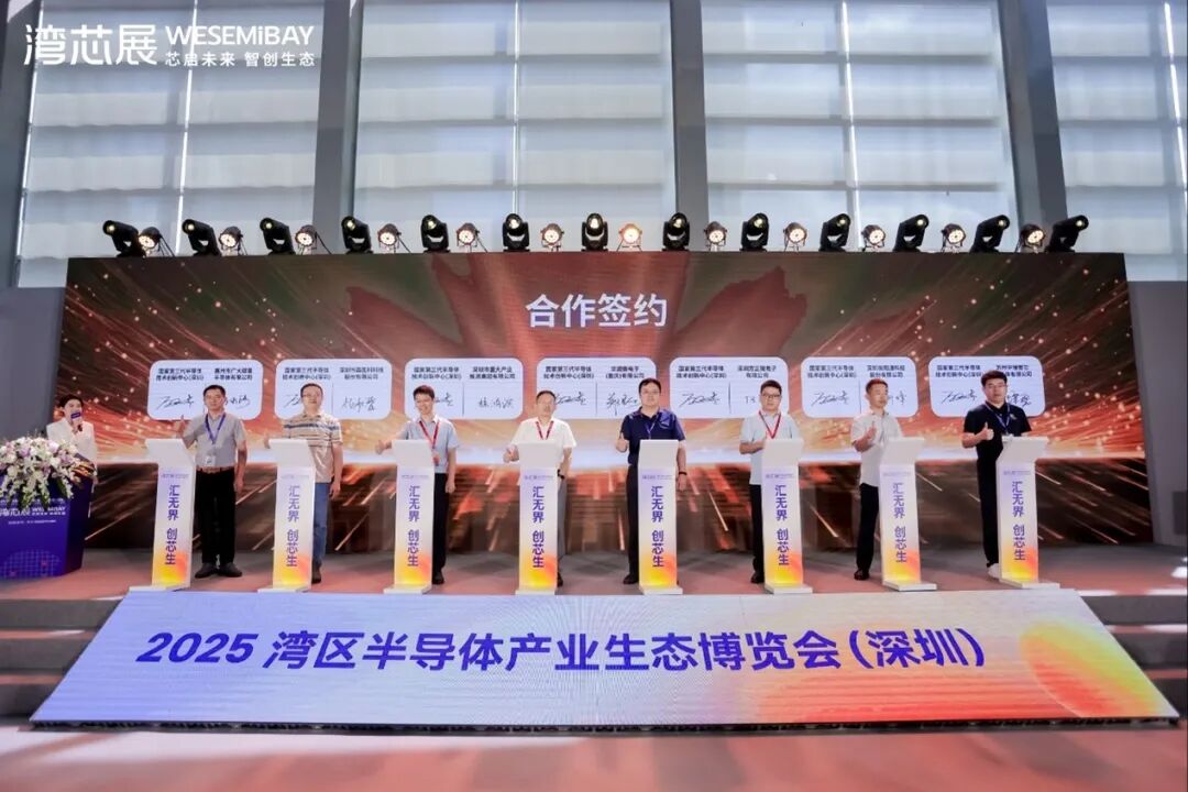
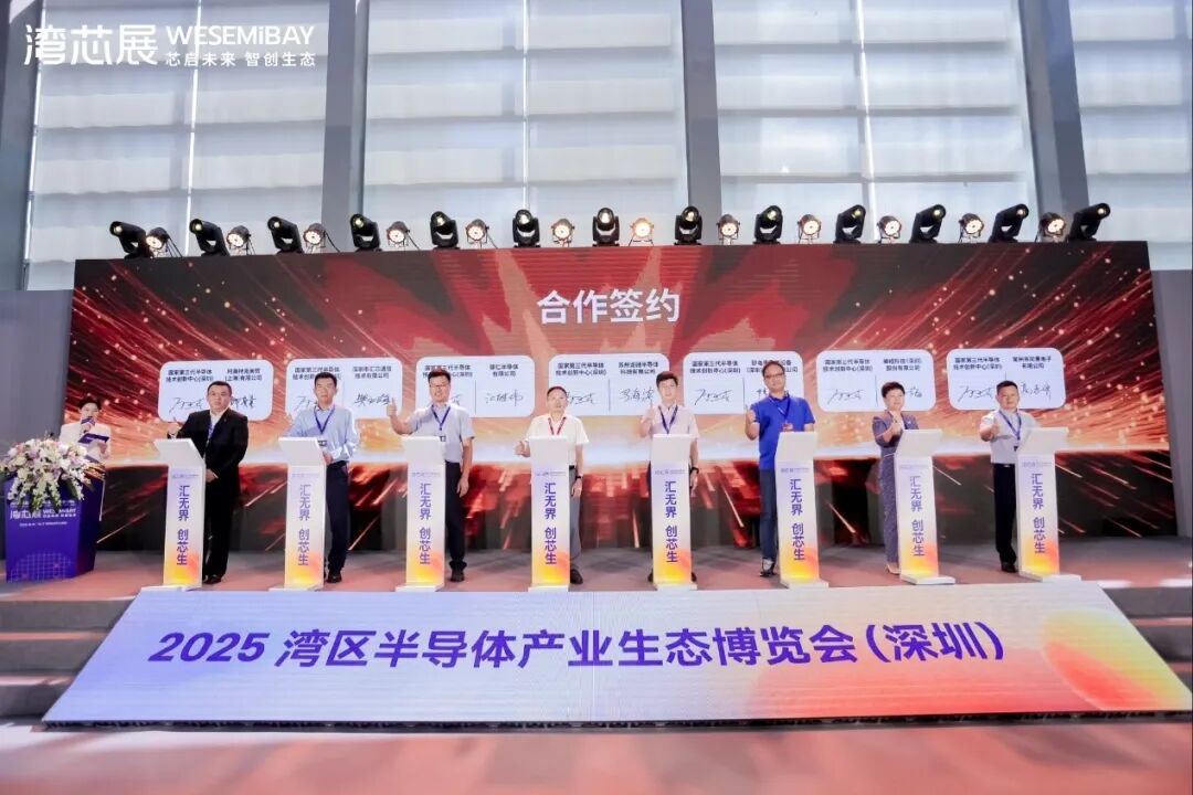
02 Cooperation Signing: Partnering with the Industrial Chain for Shared Development
Going it alone rarely leads to significant breakthroughs; collaborative innovation is the way forward. Subsequently, the Shenzhen Integrated Platform signed cooperation agreements with 14 industrial chain partners. These partnerships span multiple fields, including power semiconductor materials, devices, processes, and applications, further strengthening the industrial ecosystem and promoting the accelerated transformation of technological achievements.
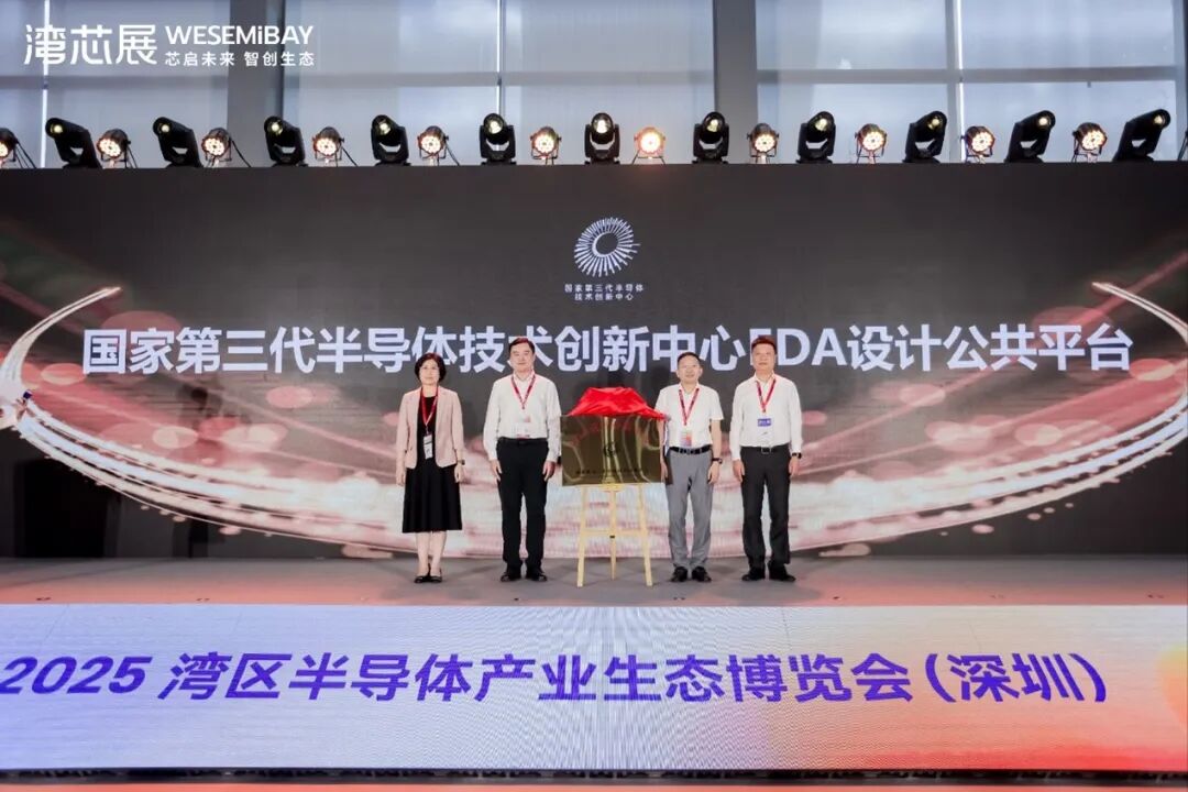
03 EDA Design Public Platform Officially Launched: Building an Independent and Controllable Design & Simulation Support System
The National Center of Technology Innovation for Wide Bandgap Semiconductor focuses on key bottlenecks in third-generation semiconductor design and tape-out verification, and has built a domestically developed EDA design public platform. Customers can use this platform for tape-out verification via the platform’s pilot production line.
At the forum, under the guidance of the Innovation Center headquarters, the Shenzhen Integrated Platform completed the signing, unveiling, and certification ceremonies for the EDA Design Public Platform, marking its official launch.
04 Release of First-of-a-Kind Domestic Process Equipment Verification Results: A Key Leap in Advancing Domestic Maturation and Validation
Jia Guojun, Deputy Director of Shenzhen Pinghu Laboratory, together with 13 domestic equipment manufacturers, including Beijing North Huachuang Microelectronics Equipment Co., Ltd., Shenzhen Han's Semiconductor Equipment Technology Co., Ltd., and Shanghai Jingce Semiconductor Technology Co., Ltd., jointly took the stage to illuminate the logos of 16 domestic equipment units. This event also marked the official release of the first-of-a-kind (set) verification results of 8-inch wide bandgap semiconductor process equipment.
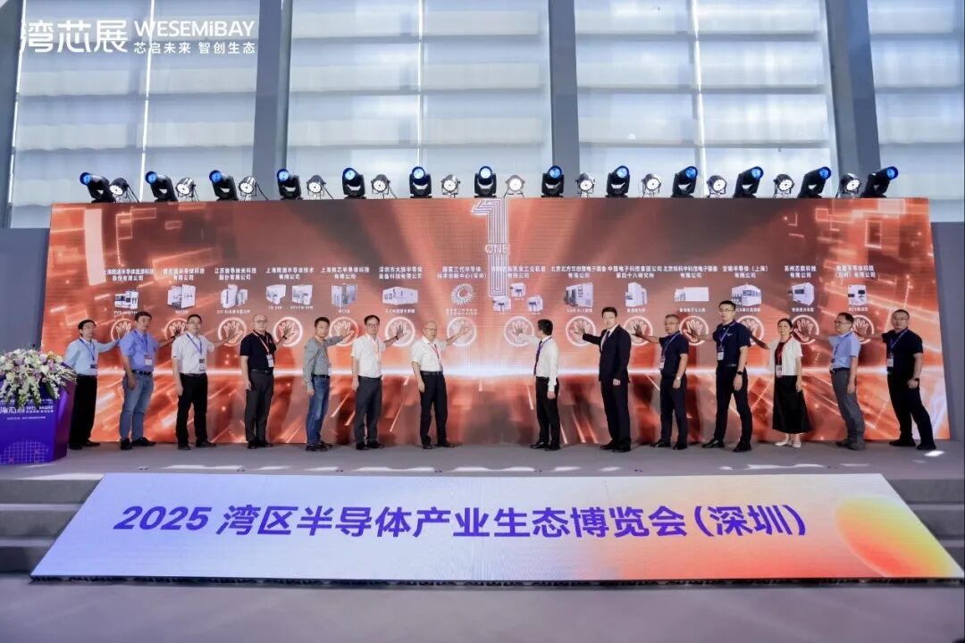
To date, the Shenzhen Integrated Platform has embraced the mission of domestic equipment verification and maturation, completing the use verification and maturation of 123 sets of high-quality domestic equipment, of which 16 sets are first-of-their-kind in niche domestic fields. Meanwhile, 96% of key materials—including target materials, specialty gases, chemicals, and photoresists—have undergone domestic verification, effectively advancing the localization of both equipment and materials.
The platform’s participation in the Bay Chip Exhibition not only showcased the substantial achievements of Technology Platform 1.0, but also highlighted its firm commitment to fostering independent control and high-quality development of China’s advanced power semiconductor industry. This was demonstrated through initiatives such as project signing, the official launch of the EDA design public platform, the release of domestic equipment verification results, and the rollout of PDK, MPW, and pilot platforms. Looking ahead, the platform will continue to uphold the principles of openness and sharing, working hand-in-hand with global industrial partners to shape a new future for the semiconductor industry.
