Paper Sharing
【Domestic Papers】Ultrahigh Performance of Self-Powered Far-UVC Detector Based on MOCVD-Grown α-Ga₂O₃ Thin Film on c-Al₂O₃ Without Any Phase Stabilizer
日期:2025-10-20阅读:514
Researchers from the Changchun Institute of Optics, Fine Mechanics and Physics, Chinese Academy of Sciences have published a dissertation titled "Ultrahigh Performance of Self-Powered Far-UVC Detector Based on MOCVD-Grown α-Ga2O3 Thin Film on c-Al2O3 Without Any Phase Stabilizer" in Journal of Alloys and Compounds.
Project Support
This work is supported by the National Natural Science Foundation of China (62574203, 12204474, 12304111, and 12304112).
Background
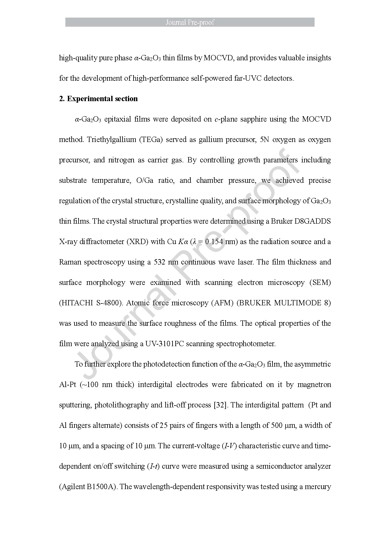
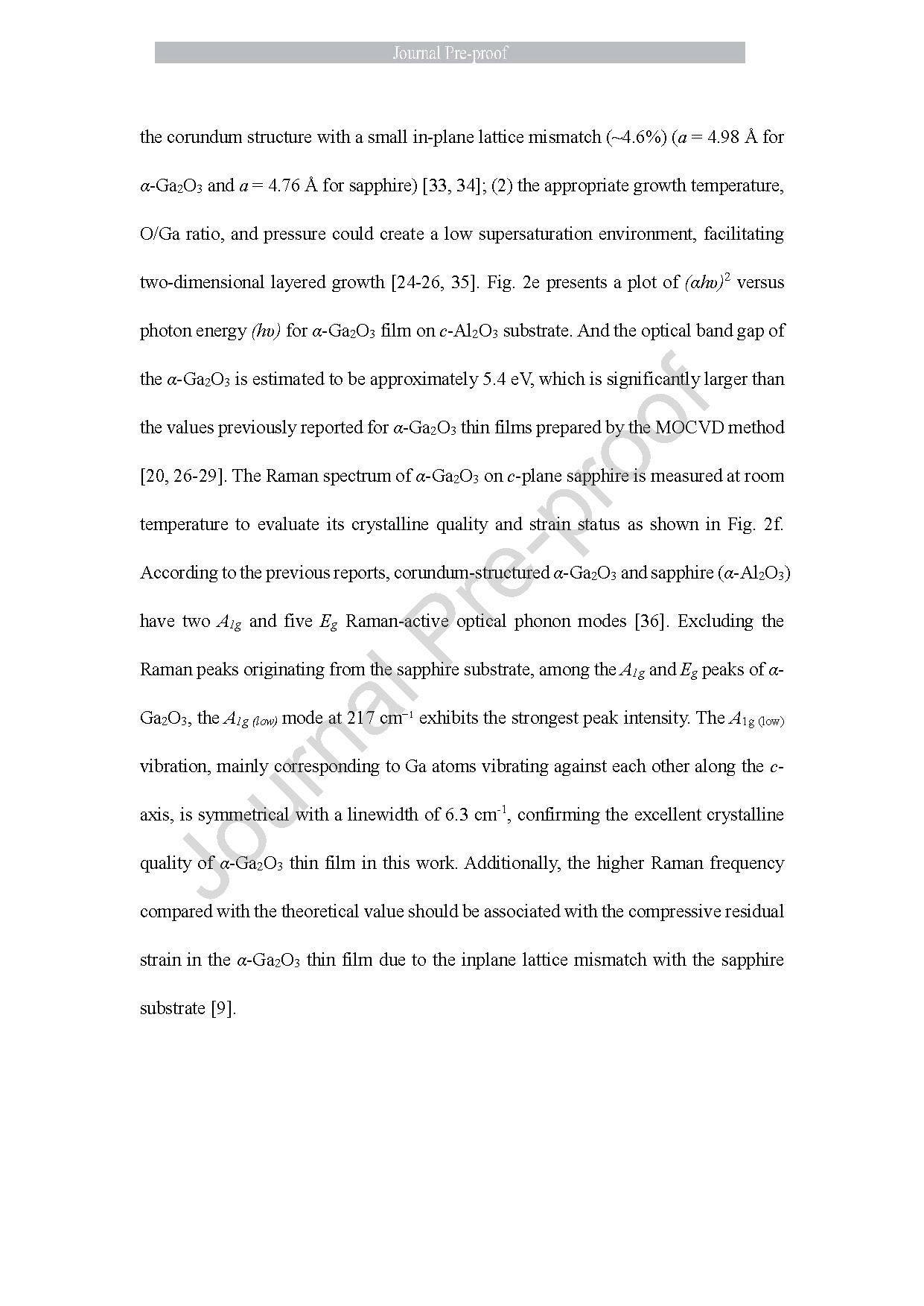
As an emerging ultrawide band gap semiconductor, α-Ga2O3, with the widest bandgap of ~5.4-5.6 eV among gallium oxide isomers, is a naturally ideal candidate material for far-ultraviolet-C (far-UVC, 200-240 nm) photodetection, offering broad application prospects in bacteria and viruses inactivation, gas monitoring (such as NO, NO2 and NH3), photo-lithography, and so on. Till now, owing to the same corundum crystal structure, α-Ga2O3 epilayers have been commonly achieved on sapphire substrates by using various methods, including mist chemical vapor deposition (Mist-CVD), halide vapor phase epitaxy (HVPE) metal-organic chemical vapor deposition (MOCVD) and pulsed laser deposition. Among these, the MOCVD method offers unique advantages, such as precise control over the film phase composition and growth rate, high purity, high uniformity, low surface roughness, and suitability for commercial mass production. However, all the reported MOCVD epitaxial growth of α-Ga2O3 films to date has required the use of sapphire substrates with specific orientations (such as m- and r-Al2O3) or the additional introduction of other sources as phase stabilizers (such as HCl and triethylboron (TEB)) during the growth process to be achieved. This not only increases the cost and complexity of the preparation, but also often leads to problems such as poor crystalline quality, a small bandgap, and phase impurities in α-Ga2O3 films. Therefore, the development of far-UVC photodetectors based on MOCVD-grown pure α-Ga2O3 films remains an unexplored frontier.
Abstract
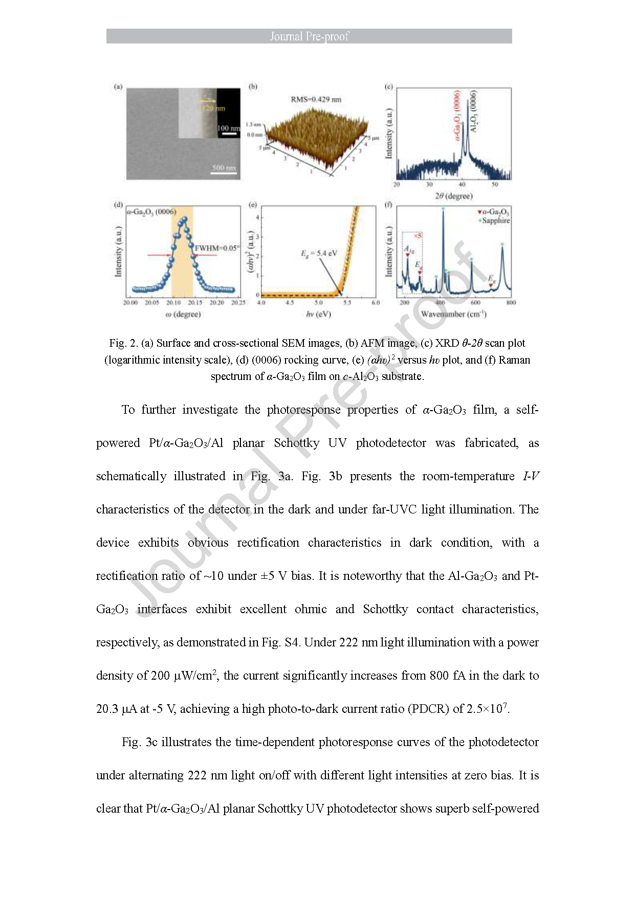
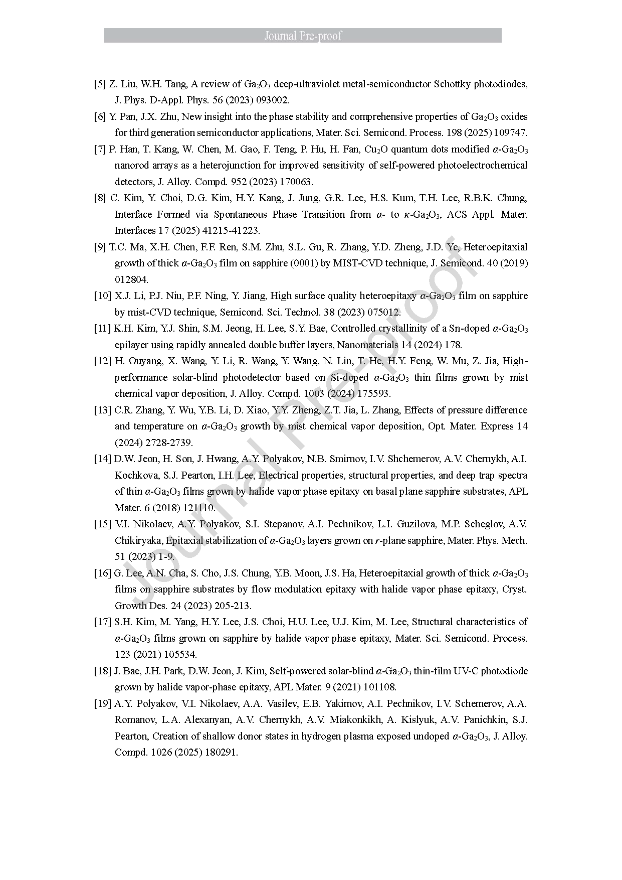
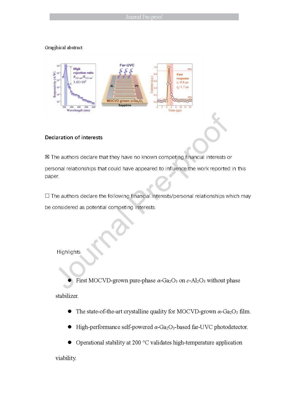
α-Ga2O3 with an ultra-wide bandgap holds significant application potential in far-ultraviolet-C (far-UVC) photodetection. Currently, the methods for epitaxial growth of α-Ga2O3 thin films via metal organic chemical vapor deposition (MOCVD) all require the use of sapphire substrates with specific orientations, or the additional introduction of phase stabilizers, which increases the complexity of preparation and affects the optoelectronic properties of the films as well as the performance of devices. In this work, high-quality pure-phase α-Ga2O3 thin films have been achieved on c-Al2O3 by using MOCVD technique without any phase stabilizer for the first time. 120 nm-thick α-Ga2O3 thin film exhibits a narrow X-ray rocking curve full width at half maximum of 0.05°, a small root-mean-square roughness of 0.429 nm, and an ultra-wide band gap of 5.4 eV, representing the best result achieved for α-Ga2O3 thin films prepared by the MOCVD method to date. Leveraging this α-Ga2O3 film, a self-powered far-UVC Pt/α-Ga2O3/Al planar Schottky photodiode was successfully developed. This device showcases a significant responsivity of 8.4 mA/W at 222 nm, an ultrafast response time of 0.8 μs and a record-high far-UVC to near-UVC rejection ratio (R222 nm/R255 nm) of 3.42×10² at room temperature under 0 V. Furthermore, the detector possesses excellent operational stability and robust resistance to high temperature of up to 200 °C. This study demonstrates a feasible approach for preparing high-quality pure-phase α-Ga2O3 thin films by MOCVD, providing valuable insights for the development of high-performance self-powered far-UVC band detectors.
Highlights
● First MOCVD-grown pure-phase α-Ga2O3 on c-Al2O3 without phase stabilizer.
● The state-of-the-art crystalline quality for MOCVD-grown α-Ga2O3 film.
● High-performance self-powered α-Ga2O3-based far-UVC photodetector.
● Operational stability at 200 °C validates high-temperature application viability.
Conclusion
In this work, a high-quality α-Ga2O3 film was firstly deposited onto c-plane sapphire substrate using the MOCVD technology without any phase stabilizer. Benefiting from the small lattice mismatch between α-Ga2O3 and c-Al2O3 as well as precise control of the growth conditions, we have obtained α-Ga2O3 epitaxial film with high crystalline quality and low surface roughness. Typically, FWHM value of the XRD rocking curve of α-Ga2O3 (0006) plane can reach as narrow as ~0.05°, representing the optimal value for α-Ga2O3 film grown by the MOCVD method. Furthermore, a self-powered far-UVC photodetector was fabricated based on this α-Ga2O3 film, demonstrating a high responsivity, an ultra-fast response speed and a large far-UVC to near-UVC rejection ratio at 0 V. The superior far-UVC photodetection performance of our device can be attributed to the high crystalline quality and the ultra-wide bandgap of α-Ga2O3 film, as well as the optimized device architecture. Meanwhile, the device also demonstrates outstanding high-temperature endurance and operational stability, highlighting the tremendous application potential of MOCVD-grown α-Ga2O3-based far-UVC photodetectors.
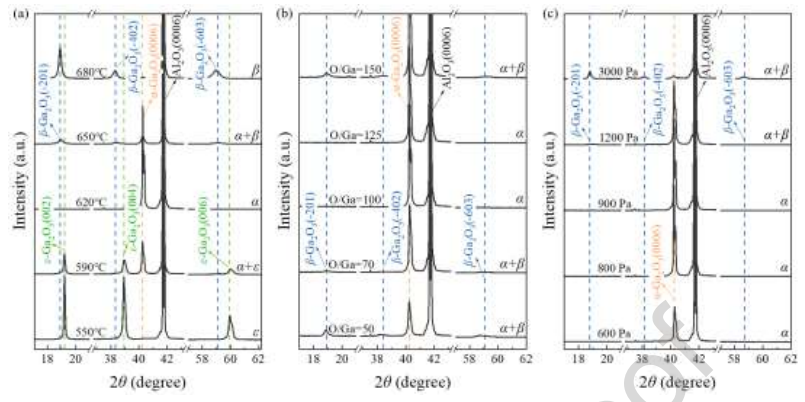
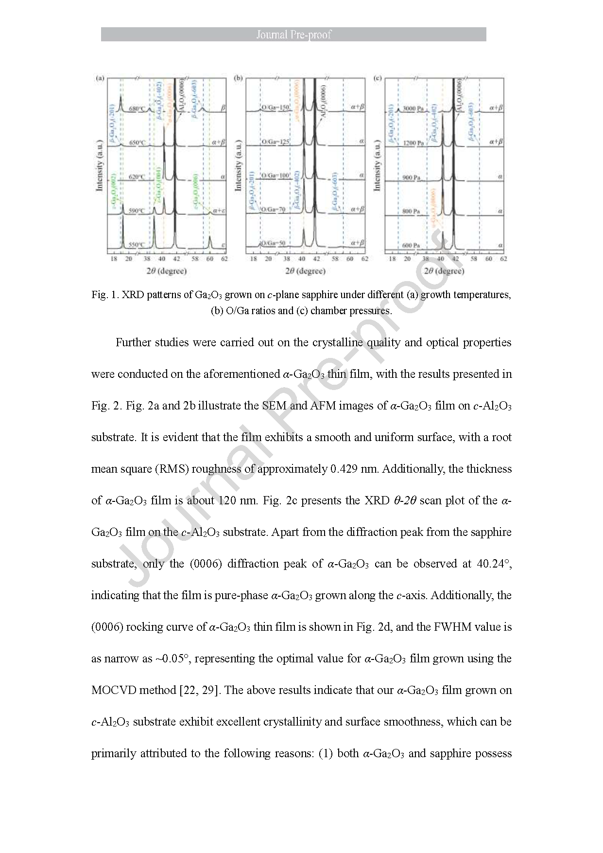
Fig. 1. XRD patterns of Ga2O3 grown on c-plane sapphire under different (a) growth temperatures, (b) O/Ga ratios and (c) chamber pressures.
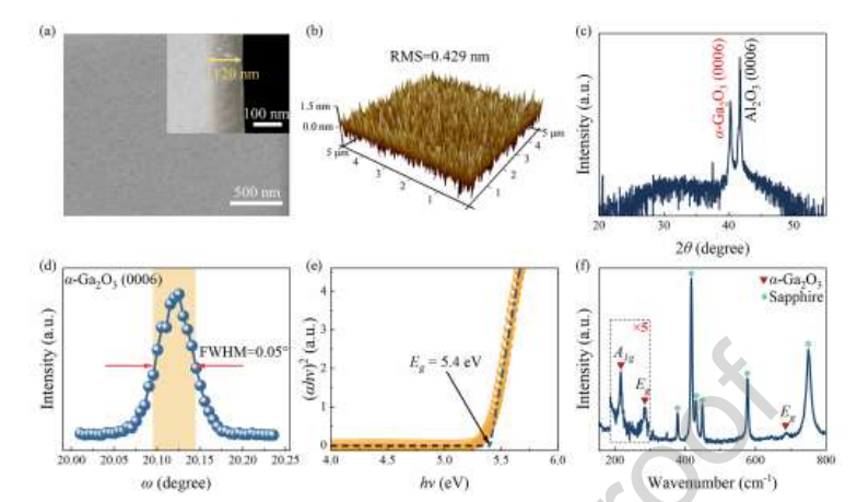
Fig. 2. (a) Surface and cross-sectional SEM images, (b) AFM image, (c) XRD θ-2θ scan plot (logarithmic intensity scale), (d) (0006) rocking curve, (e) (αhυ)2 versus hυ plot, and (f) Raman spectrum of α-Ga2O3 film on c-Al2O3 substrate.
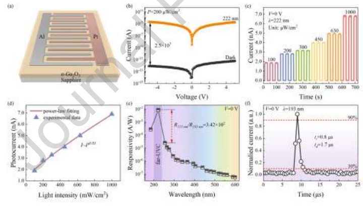
Fig. 3. (a) Schematic diagram of the structure of the Pt/α-Ga2O3/Al photodetector. (b) I-V characteristics of the device in dark and under 222 nm light illumination. (c) I-t curves under 222 nm light with different intensities at zero bias. (d) Photocurrent as a function of light intensity and the corresponding power-law fitting line. (e) Responsivity of the self-powered photodetector at different wavelengths. (f) Single-cycle transient response curve.
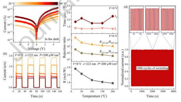
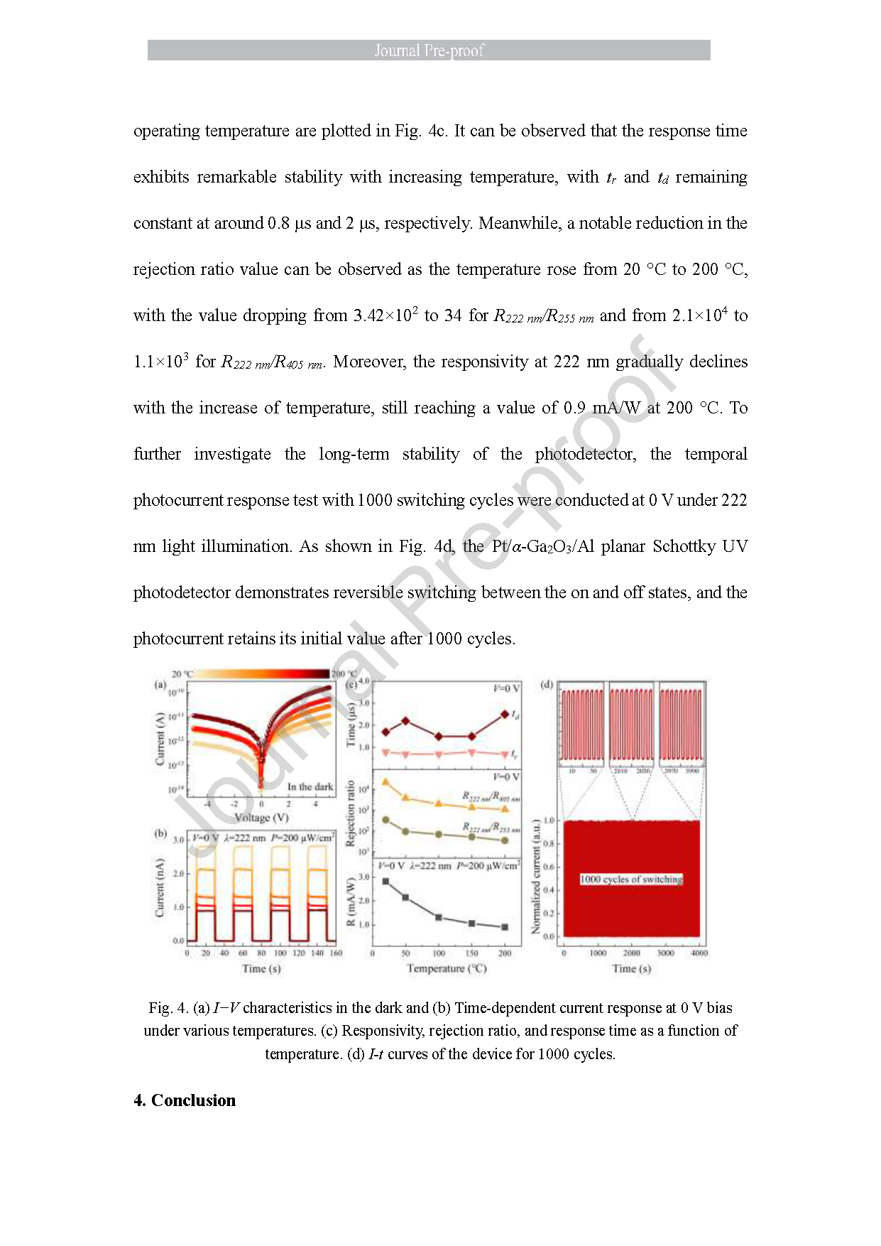
Fig. 4. (a) I−V characteristics in the dark and (b) Time-dependent current response at 0 V bias under various temperatures. (c) Responsivity, rejection ratio, and response time as a function of temperature. (d) I-t curves of the device for 1000 cycles.
DOI:
doi.org/10.1016/j.jallcom.2025.183842