Paper Sharing
【Member Papers】Variable Fluoride Ion Implantation Compound Termination in β-Ga₂O₃ Schottky Barrier Diode With Stress Test
日期:2025-10-20阅读:552
Researchers from the University of Electronic Science and Technology of China have published a dissertation titled "Variable Fluoride Ion Implantation Compound Termination in β-Ga2O3 Schottky Barrier Diode With Stress Test" in IEEE Transactions on Electron Devices.
Background
β-Ga2O3 is considered as a highly promising material for next-generation power electronics due to its wide bandgap (4.5-4.9 eV) and high critical field strength (Ecr) of 8 MV/cm. The power diodes are the critical components in power electronics. However, the electric field (E-field) concentration at the anode edge of the β-Ga2O3 diodes leads to premature breakdown. Various terminal techniques have been proposed to enhance BV, contributing to high power and high P-FOM of β-Ga2O3 diodes. Nitrogen, Helium and Magnesium ions implantation-based edge terminations were reported to suppress peak electric field (Emax) and improve the BV by forming a more-resistive region. Besides, fluorine ion (F⁻) implantation has been demonstrated as an effective termination technique. However, ion implantation into the β-Ga2O3 causes lattice damage and induces traps or defects, leading to the degradation of device reliability.
Main Content
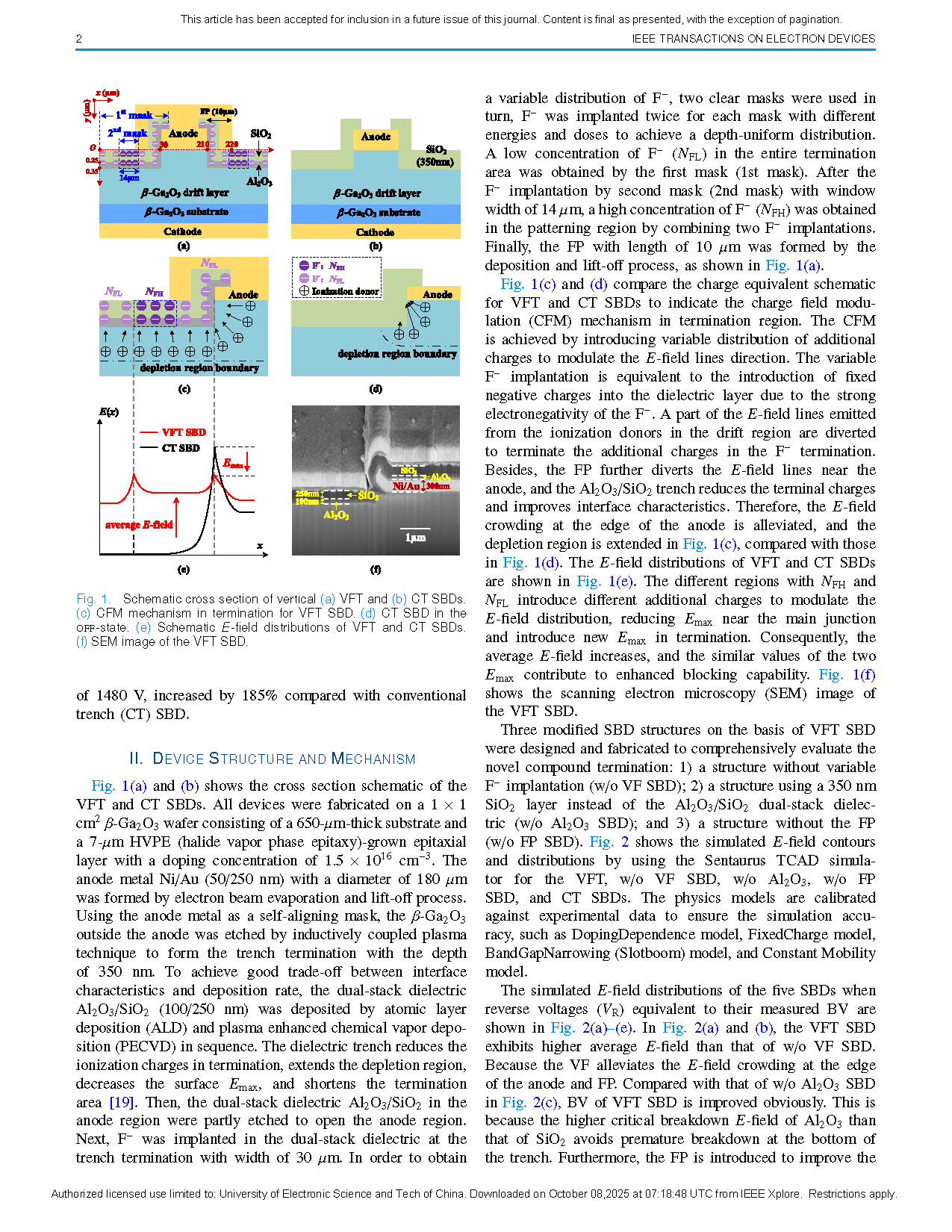
An enhanced breakdown voltage (BV) and high reliability β-Ga2O3 Schottky barrier diode (SBD) with variable fluoride ion (F⁻) implantation compound termination (VFT) is proposed and investigated by simulations and experiments. The VFT SBD features variable F⁻ implantation into the Al2O3/SiO2 trench termination with field plate (FP). First, the variation of F⁻ is equivalent to introducing variable distribution of additional charges to modulate the electric field distribution and improve BV. Second, the Al2O3/SiO2 trench reduces the charges in termination to decrease the surface electric field peak (Emax). Third, the FP further alleviates the electric field crowding at the anode edge. Thus, BV is greatly enhanced. Four, F⁻ implantation into the dielectric rather than β-Ga2O3 minimizes the lattice damage and thus reduces the induced traps or defects, contributing to high reliability.
Conclusion
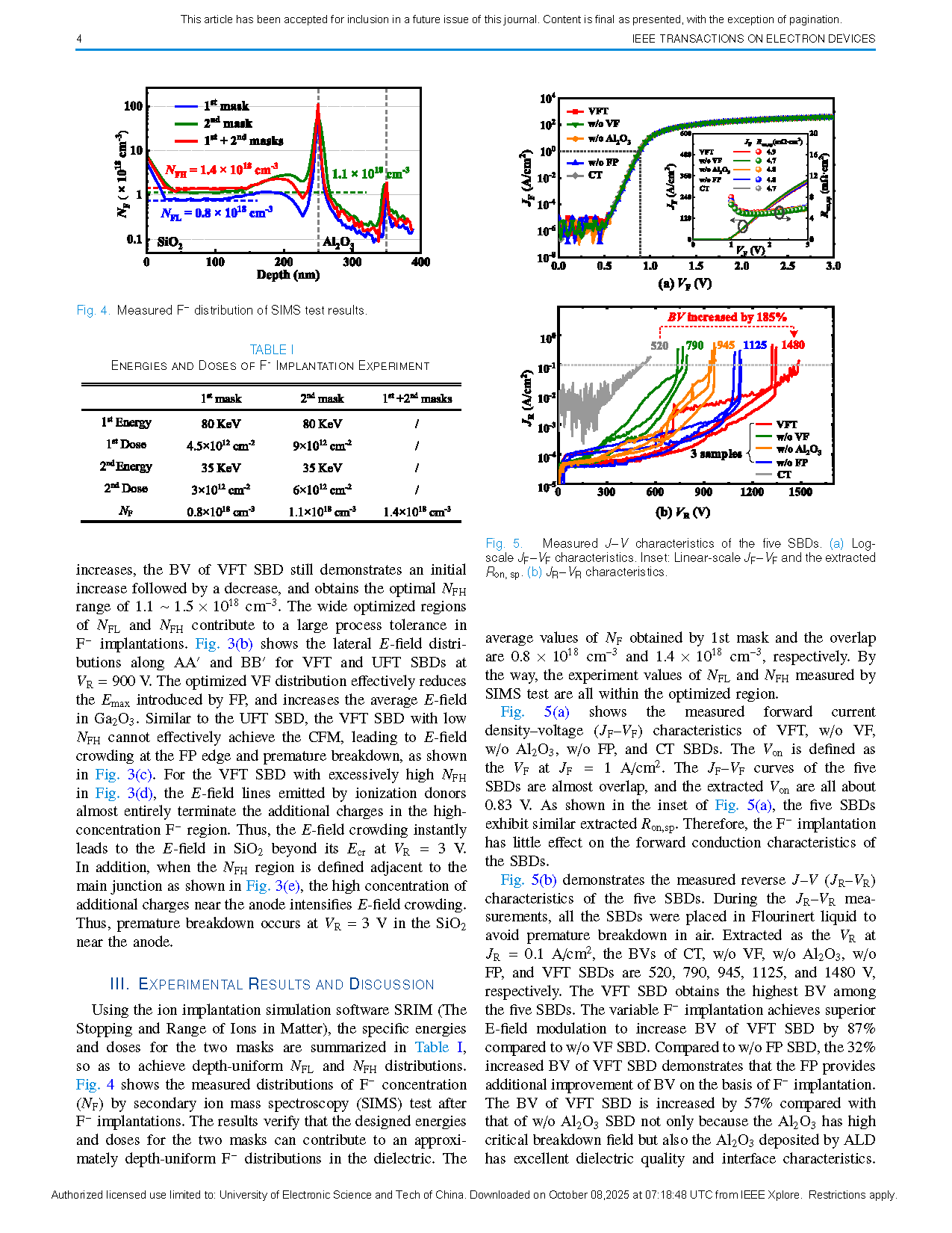
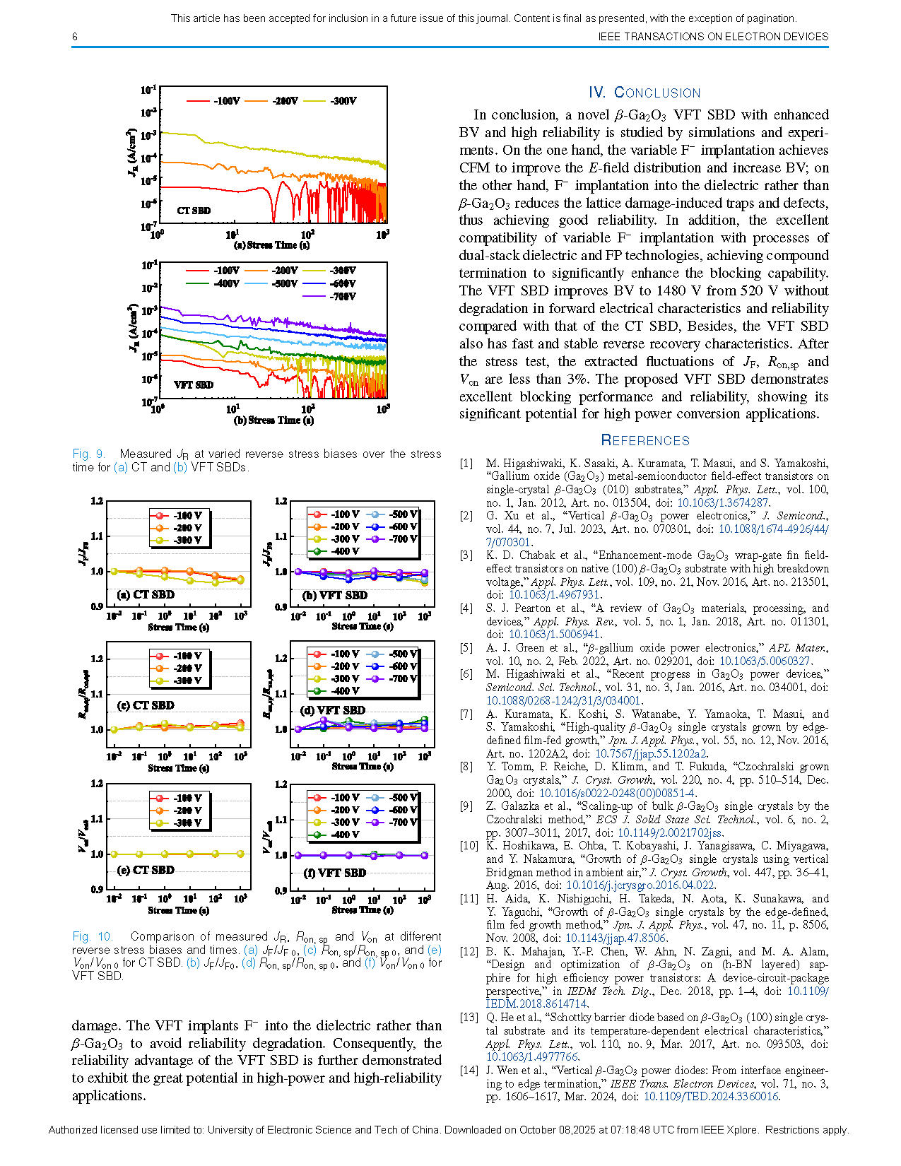
An enhanced breakdown voltage (BV) and high reliability β-Ga2O3 VFT SBD is fabricated and investigated. Compared with the SBD without F- implantation, the VFT SBD achieves high BV increasing from 520 V to 1480 V without any penalty on the forward conduction characteristics. In addition, the VFT SBD exhibits fast and stable reverse recovery characteristics. The reliability of VFT SBD is evaluated by stress test with the forward stress biases of 1, 3, 5 V and reverse stress biases applied from -100 V to -700 V. After the stress test, the fluctuations of current density, specific on-resistance and turn-on voltage are less than 3%. The fabricated VFT SBD achieves good blocking performance and reliability, showing potential in high-power and high-reliability applications.
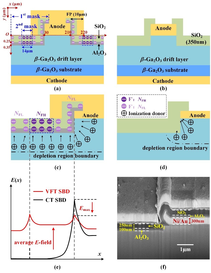
Fig. 1. Schematic cross-section of vertical (a) VFT and (b) CT SBDs. (c) Charge field modulation mechanism in termination for VFT SBD. (d) CT SBD in the off-state. (e) Schematic E-field distributions of VFT and CT SBDs. (f) SEM image of the VFT SBD.
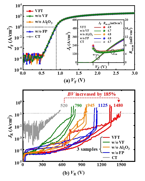
Fig. 2. Measured J–V characteristics of the five SBDs. (a) Log-scale JF–VF characteristics. Inset: Linear-scale JF–VF and the extracted Ron,sp. (b) JR–VR characteristics.
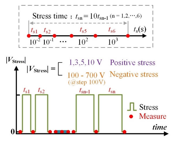
Fig. 3. Schematic representation of measure-stress-measure method.
DOI:
doi.org/10.1109/TED.2025.3614520