Paper Sharing
【International Papers】Degradation of on-current in 4 kV β-Ga₂O₃ trench Schottky barrier diodes under high voltage step stressing
日期:2025-10-21阅读:525
Researchers from the University of Bristol have published a dissertation titled "Degradation of on-current in 4 kV β-Ga2O3 trench Schottky barrier diodes under high voltage step stressing" in Applied Physics Letters.
Background
β-Ga2O3 has opened promising avenues for electric transportation, power conversion, power grids, and beyond. It has been predicted that Ga2O3 could potentially replace SiC in medium and high voltage DC power converters. However, the lack of p-type doping and conductivity in Ga2O3 has restricted the device structures to be limited to unipolar Schottky diodes, while bipolar structures require heterogenous integration with p-NiOx. The high leakage current due to the peak electric field at the Schottky interface has impeded Schottky diodes to be truly usable in ampere-class kV devices. Trench Schottky barrier diode (TSBD) is an advanced structure that utilizes fins with sidewall MOS capacitors to reduce the surface electric field (RESURF) by moving the peak electric field into the bulk of fins away from the device surface. The RESURF effect significantly curtails the reverse leakage current while simultaneously achieving good breakdown voltages; up to 2.9 kV have been reported to date using field-plate edge terminations, predominantly with failure of the dielectric layer at the corner of the fins. The sidewall dielectric interface with Ga2O3 and the fin orientation impact the current conduction capabilities as a result of charges trapping at the interface as observed under forward bias stressing conditions. There are only very limited reliability studies reported on this device system under high reverse stressing conditions, important for their future industrialization.
Abstract
Reliability of β-Ga2O3 based trench Schottky barrier diodes with a breakdown voltage of 4 kV and a Baliga's figure of merit of ∼1 GW/cm2 is reported. The devices were stressed with reverse voltages up to 3 kV in increasing steps of 250 V, followed by an evaluation of the on-state characteristics after each step-stress. The step-stress testing revealed an increase in on-state resistance of <3% when stressed up to 2.25 kV but degrades to 13% when stressed at 3 kV, recovering fully after 3 h rest time. The degradation in on-state characteristics (current collapse) under high reverse bias stress is attributed to the negative charge trapping near the bottom corner of the fins, which reduces the net conductive area of the fins. The current degradation could be replicated through drift-diffusion simulations, with trapped charge density of ∼3 × 1012 cm−2 required to match 13% degradation observed experimentally. This work highlights the critical influence of dielectric properties and charge trapping on the reliability and performance of ultra-wide bandgap materials like Ga2O3.
Conclusion
In summary, trench Schottky barrier diodes with a breakdown voltage of 4 kV and Baliga's power FOM of ∼1 GW/cm2 are demonstrated, and their behavior under short-term stress was studied. The diodes were step-stressed at reverse bias conditions up to 3 kV with post-stress on-characteristics at each step measured revealing a small decrease in on-current with increasing stress voltage. The extracted degradation in on-resistance was less than 3% up to 2.25 kV and 13% with a stress voltage of 3 kV—highlighting the potential of Ga2O3 based devices in reliable high voltage applications. The cause of degradation is pin-pointed to the injection of charges around the corner of trenches under high electric field, rather than being limited by the Ga2O3 itself. The stored charges then modulate the depletion region during on-state measurements and decrease the net conduction area causing increase in on-resistance. This study highlights the impact of high-voltage stress on the performance of β-Ga2O3 trench Schottky barrier diodes, providing insights into the mechanisms driving device degradation.
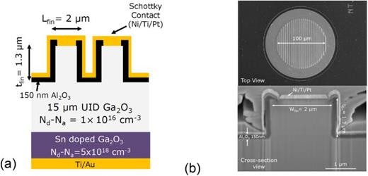
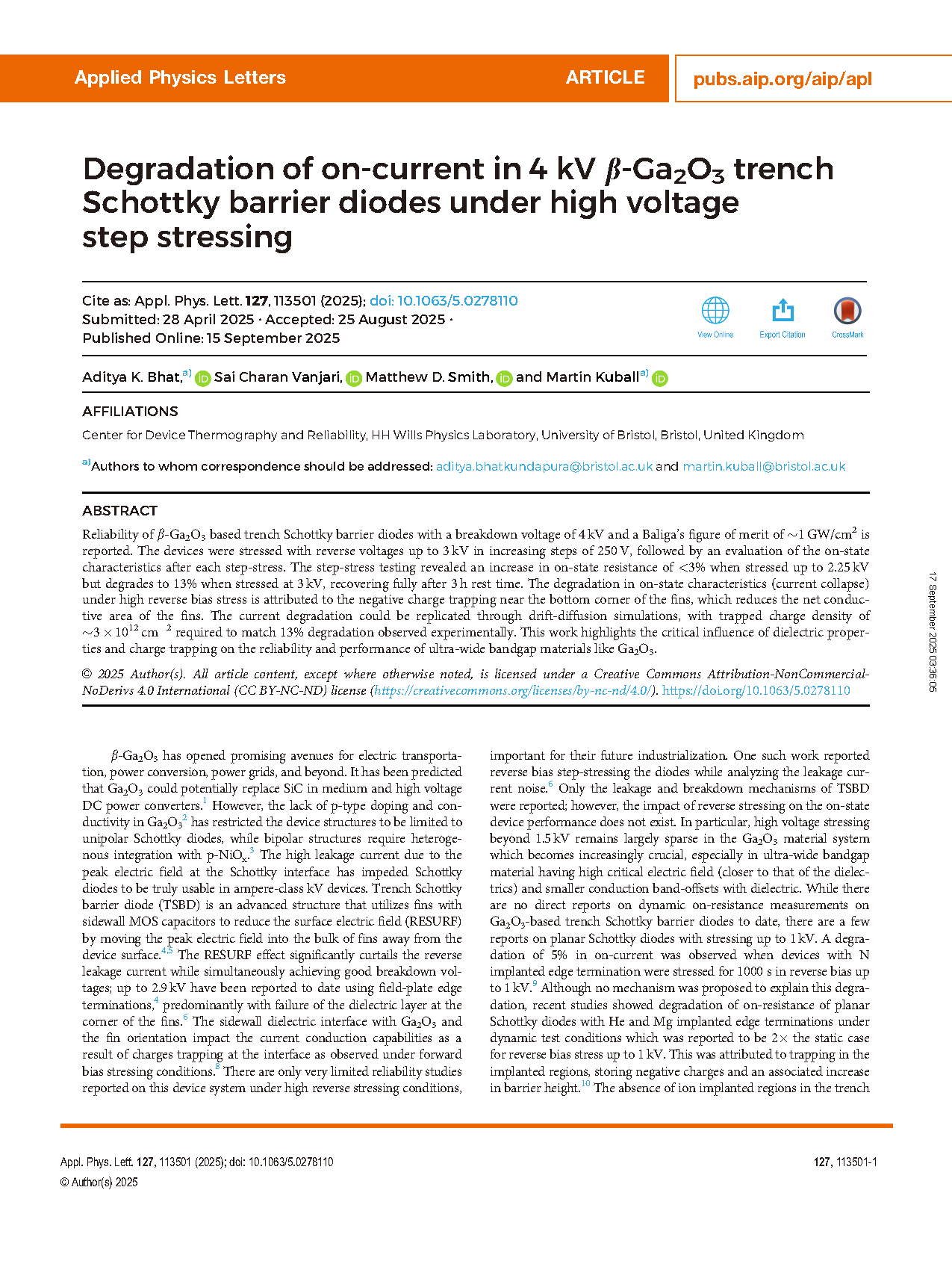
FIG. 1. (a) Cross-sectional schematic of Ga2O3 TSBD. (b) Top view and cross-sectional SEM view of the TSBD.
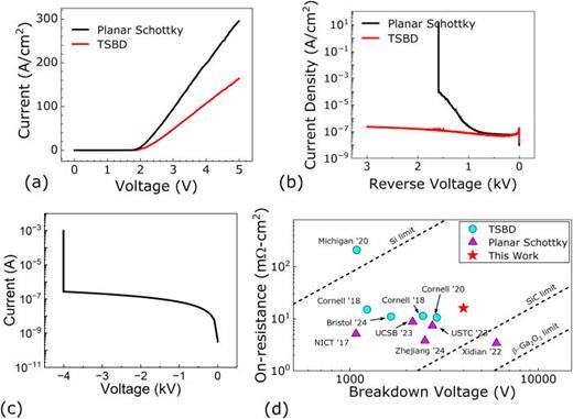
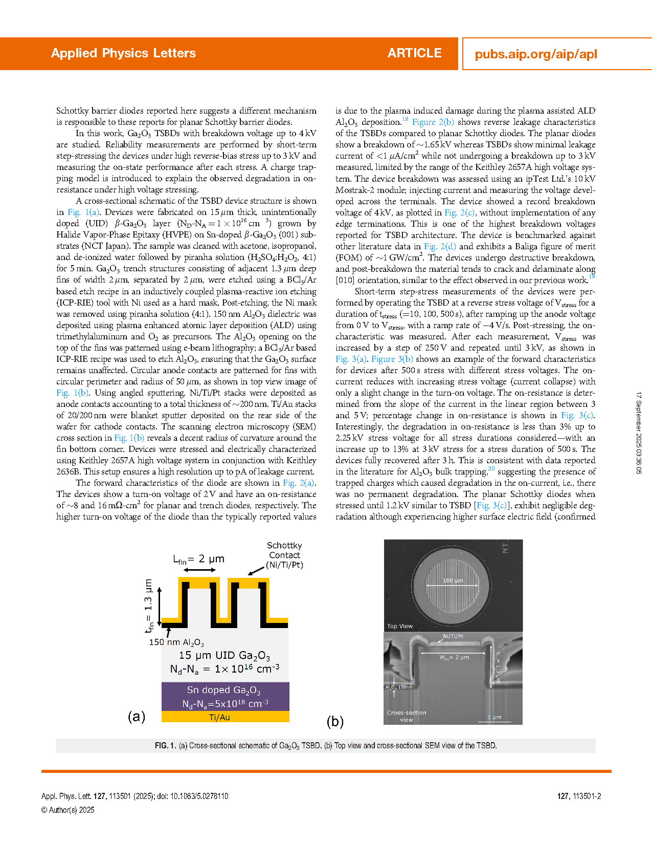
FIG. 2. (a) Forward characteristics of the diode; (b) reverse characteristics up to 3 kV. The breakdown of TSBD was above 3 kV; (c) breakdown characteristics measured using 10 kV setup with TSBD showing breakdown of 4 kV by injecting current and measuring the voltage; (d) figure-of-merit plot for TSBD fabricated in this work benchmarked against literature reports.
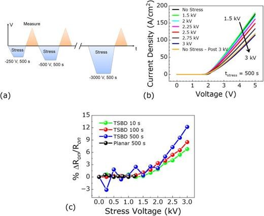
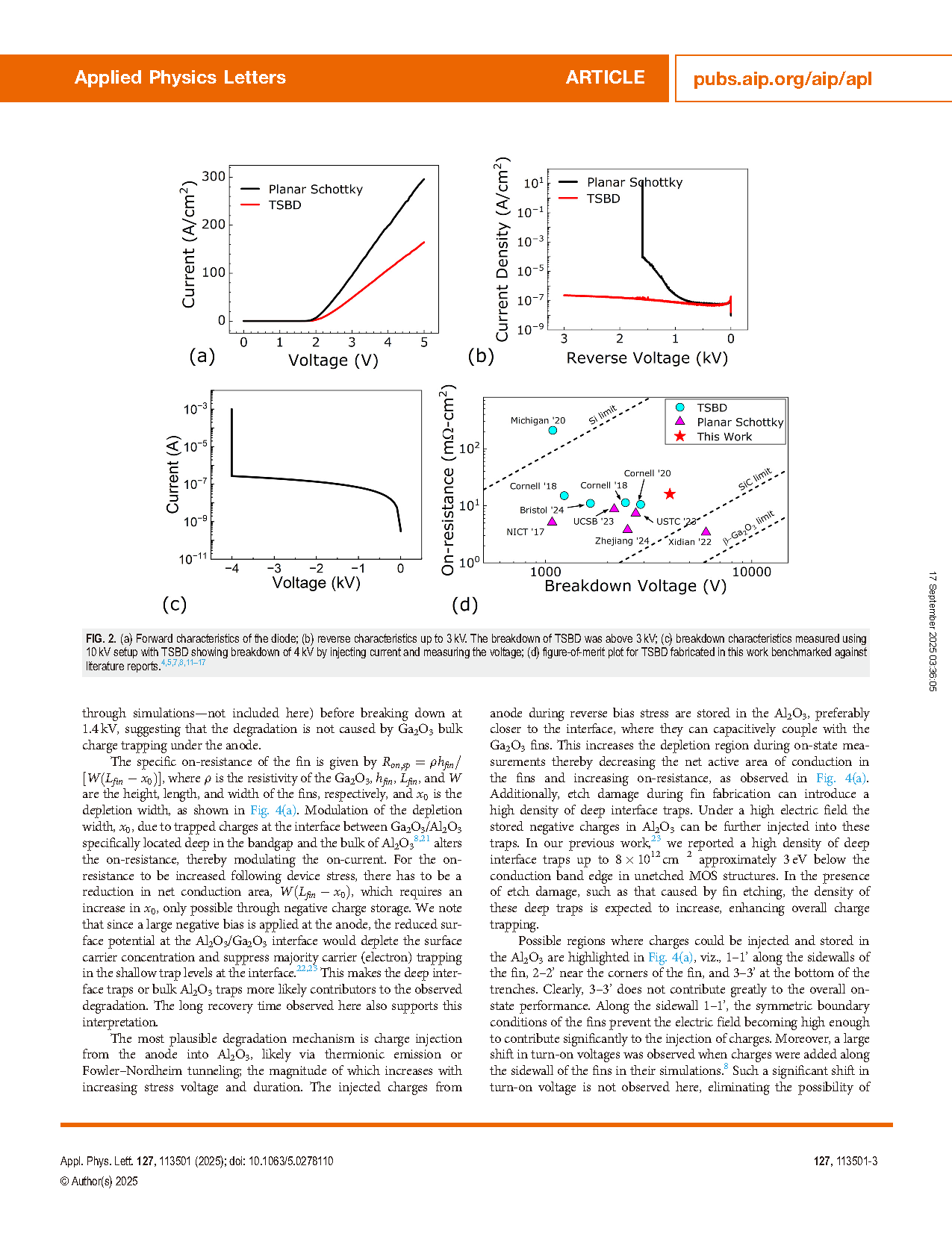
FIG. 3. (a) Time scale representation of the reliability measurements; (b) on-characteristics of the diode after 500 s stress at different stress voltages; (c) percentage increase in on-resistance (Ron) after each stress voltage in comparison with planar diodes.
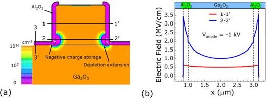
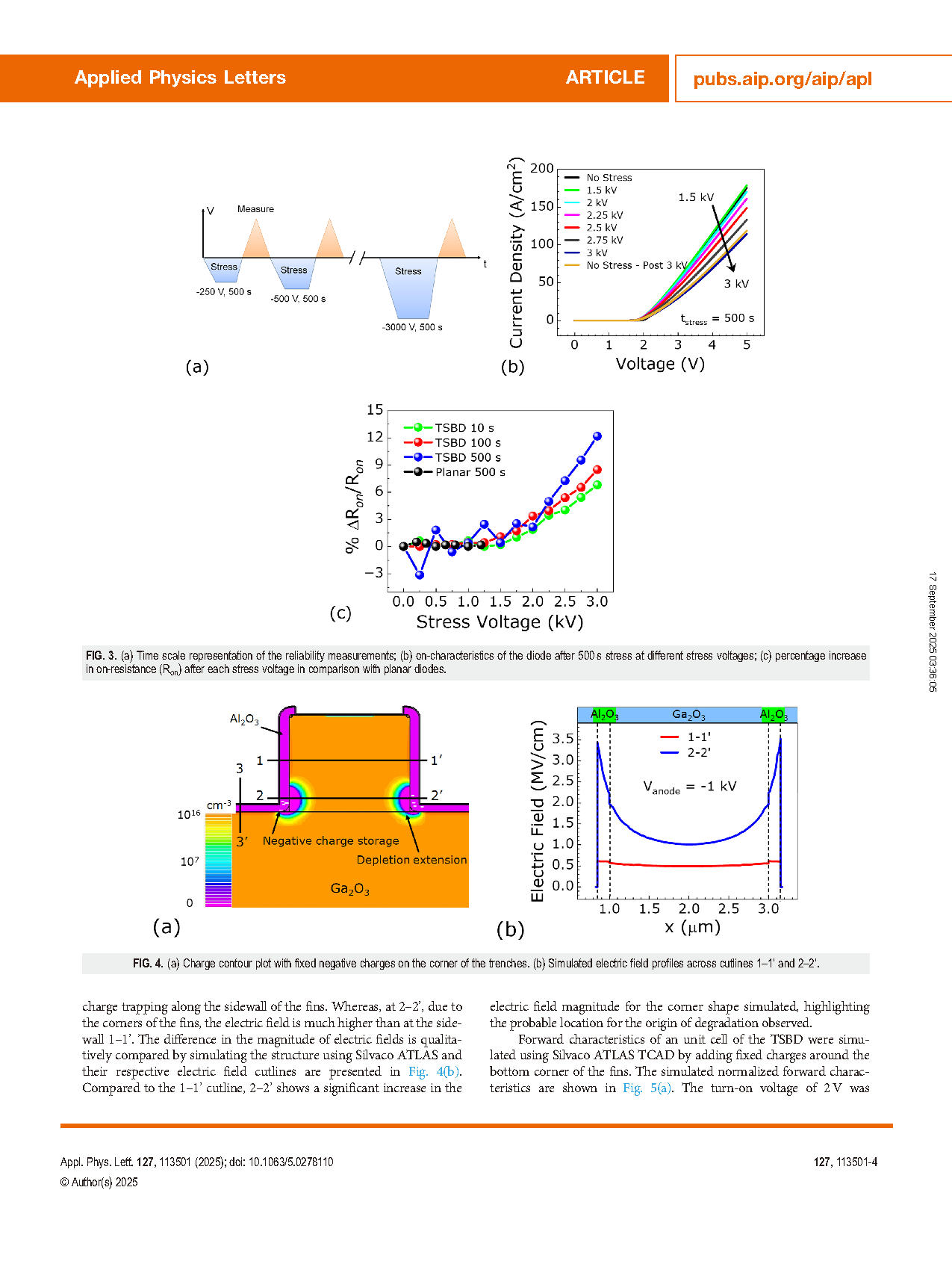
FIG. 4. (a) Charge contour plot with fixed negative charges on the corner of the trenches. (b) Simulated electric field profiles across cutlines 1–1' and 2–2'.
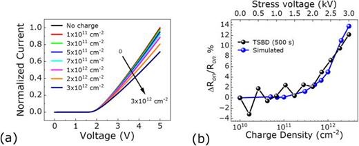
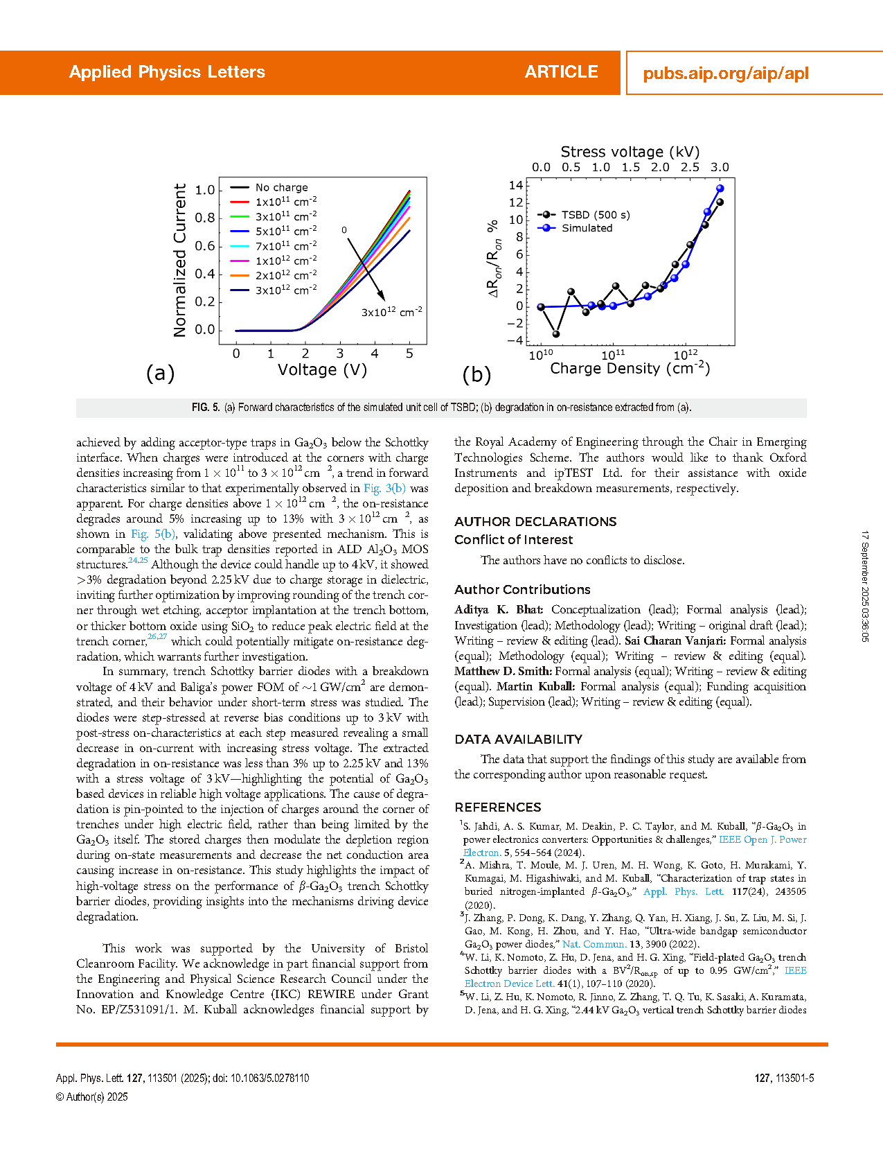
FIG. 5. (a) Forward characteristics of the simulated unit cell of TSBD; (b) degradation in on-resistance extracted from (a).
DOI:
doi.org/10.1063/5.0278110