


Paper Sharing
【Member Papers】Thermal Oxidation–Enabled β-Ga₂O₃/GaN Heterojunction for Broadband Self-Powered UV Detection
日期:2025-10-21阅读:641
Researchers from the Chongqing Normal University have published a dissertation titled "Thermal Oxidation–Enabled β-Ga₂O₃/GaN Heterojunction for Broadband Self-Powered UV Detection" in Optics Letters.
Abstract
We report a self-powered broadband UV photodetector based on a β-Ga2O3/GaN heterojunction formed via one-step thermal oxidation. The device exhibits high responsivities of 153.9 mA/W (254 nm, 300 μW/cm2, 0 V) and 52.3 mA/W (365 nm, 300 μW/cm2, 0 V), with excellent detectivity (1.25 × 10¹² Jones) and fast response (189 ms/96 ms). The type-I band alignment and low interfacial trap density enable efficient carrier separation. Single-pixel imaging of characters and patterns under UVA and UVC illumination further demonstrates its application potential. This work provides a viable route for high-performance, self-powered broadband UV photodetectors using thermal oxidation.
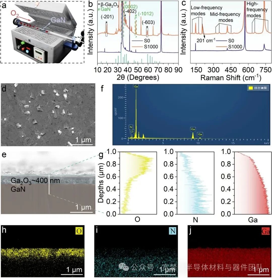
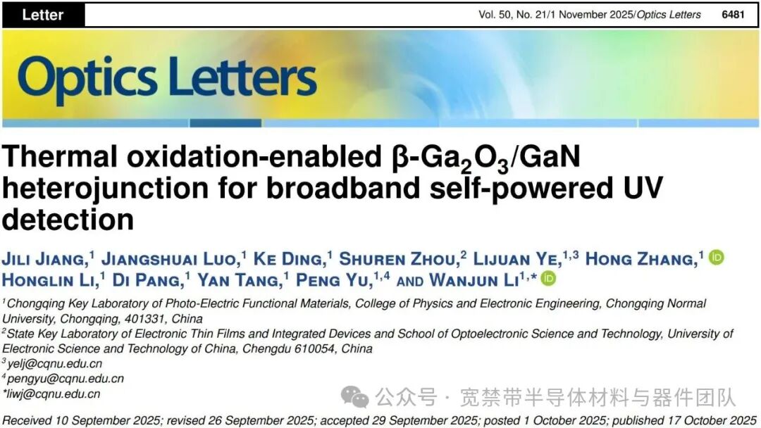
Fig. 1. (a) Thermal oxidation of a GaN thin film in a tube furnace. (b) XRD of S0 (pre-oxidation) and S1000 (oxidized at 1000 °C). (c) Raman spectra of S0 and S1000. (d, e) Surface and cross-sectional SEM of S1000. (f) EDS spectra of S1000. (g–j) Line-scan profiles and elemental maps of O, N, and Ga in the cross-section of S1000.
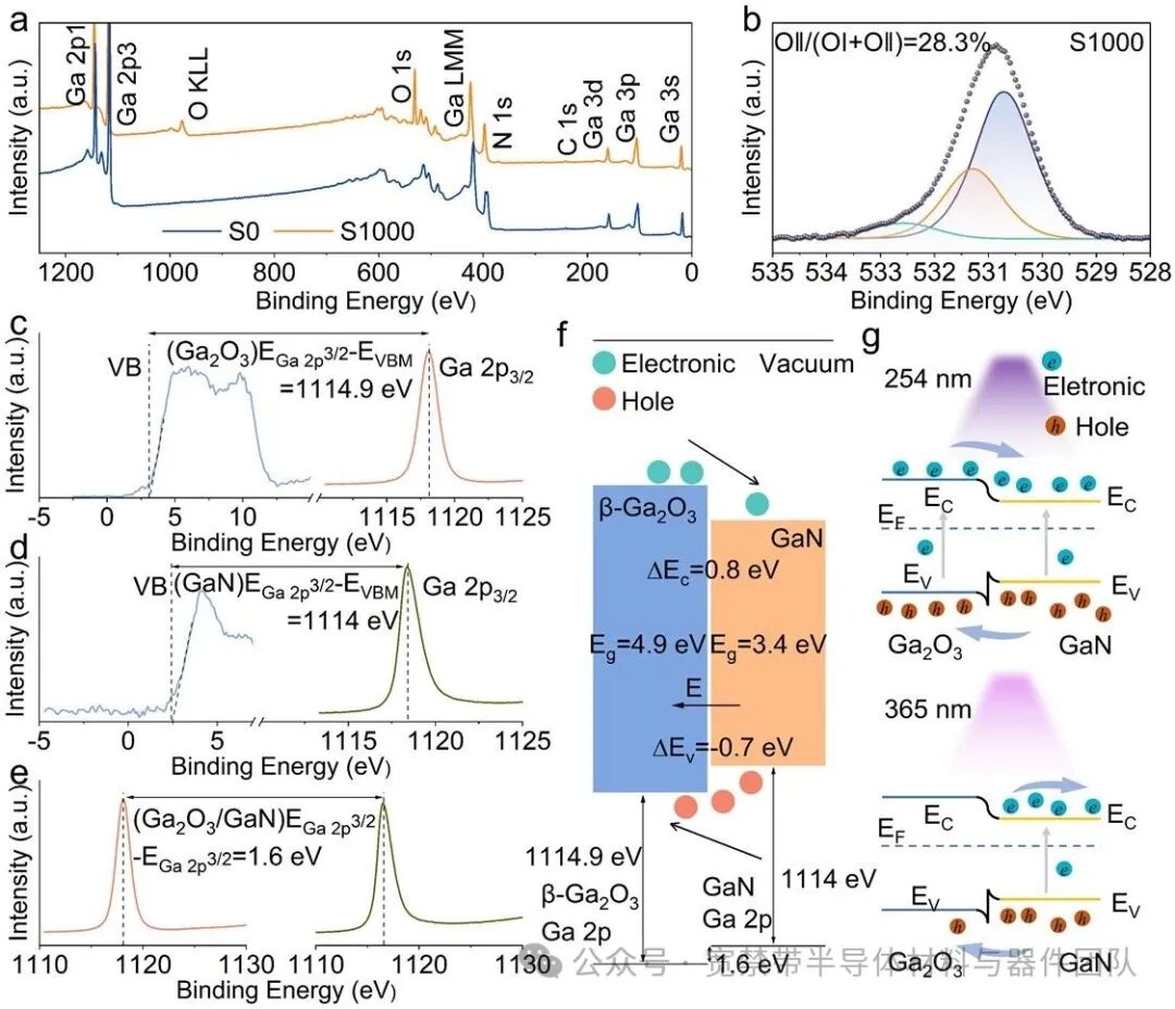
Fig. 2. (a) XPS survey of S0 and S1000. (b) O 1s spectrum of S1000 with peak fitting. (c) Ga 2p3/2 and valence band spectra of S1000. (d) Ga 2p3/2 and valence band spectra of S0. (e) Ga 2p3/2 spectra of S0 and S1000. (f) Band alignment diagram of the β-Ga2O3/GaN heterojunction. (g) Carrier transport mechanisms under 254 and 365 nm UV illumination.
Fig. 3. (a) Schematic of the self-powered Ga2O3/GaN heterojunction photodetector. (b) Spectral responsivity at 0 V. (c) I–V curves under 254 nm illumination with varying power densities. (d) I–V curves under 365 nm illumination with varying power densities. (e) Power-law fitting of photocurrent versus power density at 254 and 365 nm (0 V). (f) I–T curve under 254 nm at 0 V. (g) I–T curve under 365 nm at 0 V.
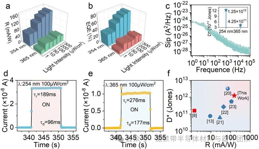
Fig. 4. (a)-(b) R and EQE under 254 nm and 365 nm illumination. (c) Noise power spectral density; the inset (top right) shows the calculated D* derived from the noise spectrum. (d)-(e) Temporal response (rise/fall time) under 254 nm and 365 nm illumination, respectively. (f) Comparison of R and D* for comparable photodetectors.
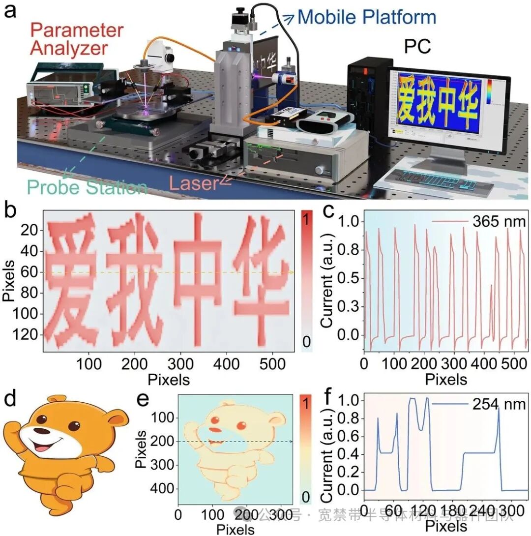
Fig. 5. (a) Schematic of the device integrated into a single-pixel imaging system. (b) Imaging of the Chinese characters “爱我中华” under 365 nm UV. (c) Photocurrent profile during horizontal scanning at the 60th vertical pixel under 365 nm UV illumination. (d) Imaging of a bear-shaped pattern under 254 nm UV. (e) Photocurrent profile during horizontal scanning at the 200th vertical pixel under 254 nm UV illumination.
DOI:
https://doi.org/10.1364/OL.578462
