Paper Sharing
【Domestic Papers】Theoretical study on interfacial tuning via Ga/Zn mutual cation doping: Mechanism in Ga₂O₃/ZnO heterojunctions
日期:2025-10-22阅读:517
Researchers from the Inner Mongolia University of Technology have published a dissertation titled "Theoretical study on interfacial tuning via Ga/Zn mutual cation doping: Mechanism in Ga2O3/ZnO heterojunctions" in Chemical Engineering Journal.
Project Support
This work was supported by the National Natural Science Foundation of China (Grant No. 12164031), the Natural Science Foundation of Inner Mongolia (Grant Nos. 2023LHMS01004, NJZY22376 and JY20250043).
Background
β-Ga2O3 possesses a wide range of applications in photodetectors due to the wide band-gap of 4.9 eV, high breakdown electric field of 6–8 MV/cm, short absorption cutoff edge, excellent stability, ease of preparation, and low loss. The desirable band-gap of β-Ga2O3 enhances its absorption properties in the solar-blind ultraviolet (UV) region, where solar-blind UV light is absorbed by the ozone layer and is almost absent at the Earth's surface. Therefore, β-Ga2O3 exhibits unique characteristics of low background noise and high sensitivity, making it widely used in applications such as environmental monitoring, space communication, missile tracking, and biomedical research Currently, Metal-Semiconductor (MS) and Metal-Semiconductor-Metal (MSM) structures are much commonly used for β-Ga2O3-based solar-blind UV detectors, with MSM β-Ga2O3 detectors already in commercial operation. However, these detectors suffer from continuous photoconductivity, slow response times, and the need for an external power supply to operate. The response speed of optoelectronic devices is primarily affected by the mobility and recombination rates of charge carriers. Therefore, improving the mobility and recombination speed of charge carriers is a key challenge in optimizing β-Ga2O3 based optoelectronic devices.
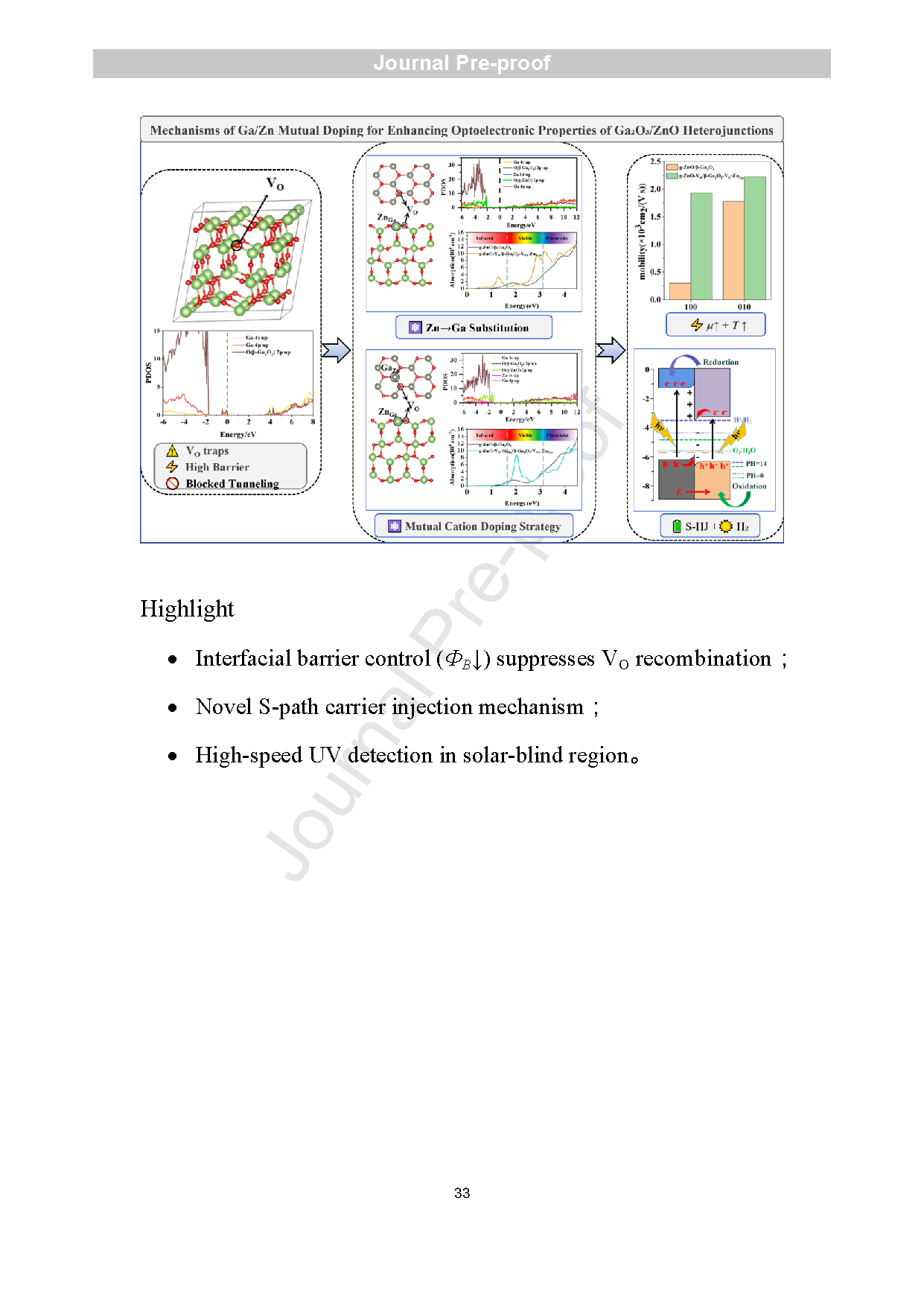
Therefore, in this work, the photoelectric properties of g-ZnO/β-Ga2O3 heterojunctions were systematically investigated. In particular, the mechanism by which the introduction of intrinsic defects such as VO, GaZn, and ZnGa modulate the photoelectric behavior of the heterojunctions were examined. This doping strategy enabled the fabrication of heterojunction optoelectronic devices with enhanced performance, thereby providing a theoretical foundation for the design of high-efficiency optoelectronic systems.
Abstract
The ultra-wide band-gap of β-Ga2O3 makes it highly suitable for solar-blind UV detection. However, intrinsic oxygen vacancies (VO) hinder its performance by acting as recombination centers and obstructing carrier transport. We demonstrate that g-ZnO/β-Ga2O3 heterojunctions, with controlled GaZn (Ga → Zn) and ZnGa (Zn → Ga) doping, can mitigate these limitations. GaZn doping reduces the n-type conductivity of g-ZnO, reduces the Schottky barrier height, and increases the dielectric response, while ZnGa doping improves the n-type conductivity of β-Ga2O3 and lowers interfacial barriers, resulting in an 80.8 % tunneling probability, an increase in charge transfer, and a more than 7-fold improvement in mobility. Co-doping establishes an S-shaped charge transfer pathway through HOMO electron-valence band hole recombination, enhancing conductivity compared to undoped structures. The heterostructure exhibits strong UV absorption in the 200–300 nm range, along with improved responsivity. These results present a doping strategy for high-performance β-Ga2O3 photodetectors, particularly for solar-blind applications that demand fast response time and low dark current.
Highlights
● Interfacial barrier control (ΦB↓) suppresses VO recombination.
● Novel S-path carrier injection mechanism
● High-speed UV detection in solar-blind region
Conclusion
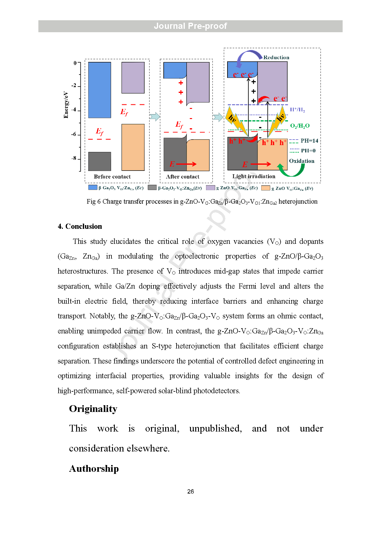
This study elucidates the critical role of oxygen vacancies (VO) and dopants (GaZn, ZnGa) in modulating the optoelectronic properties of g-ZnO/β-Ga2O3 heterostructures. The presence of VO introduces mid-gap states that impede carrier separation, while Ga/Zn doping effectively adjusts the Fermi level and alters the built-in electric field, thereby reducing interface barriers and enhancing charge transport. Notably, the g-ZnO-VO:GaZn/β-Ga2O3-VO system forms an ohmic contact, enabling unimpeded carrier flow . In contrast, the g-ZnO-VO:GaZn/β-Ga2O3-VO:ZnGa configuration establishes an S-type heterojunction that facilitates efficient charge separation. These findings underscore the potential of controlled defect engineering in optimizing interfacial properties, providing valuable insights for the design of high -performance, self-powered solar-blind photodetectors.
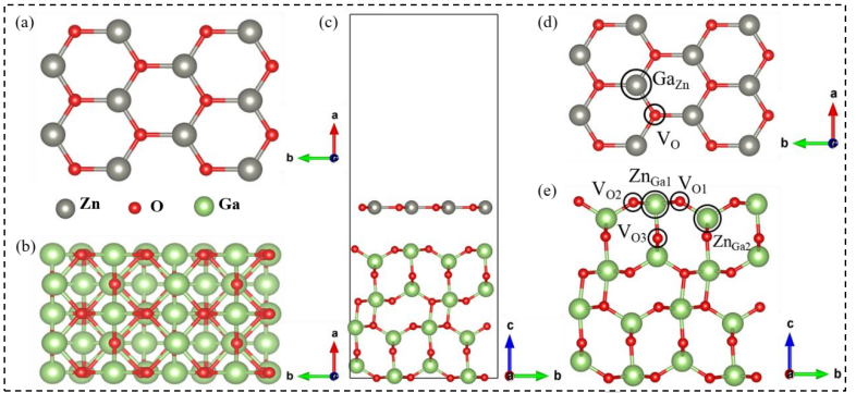
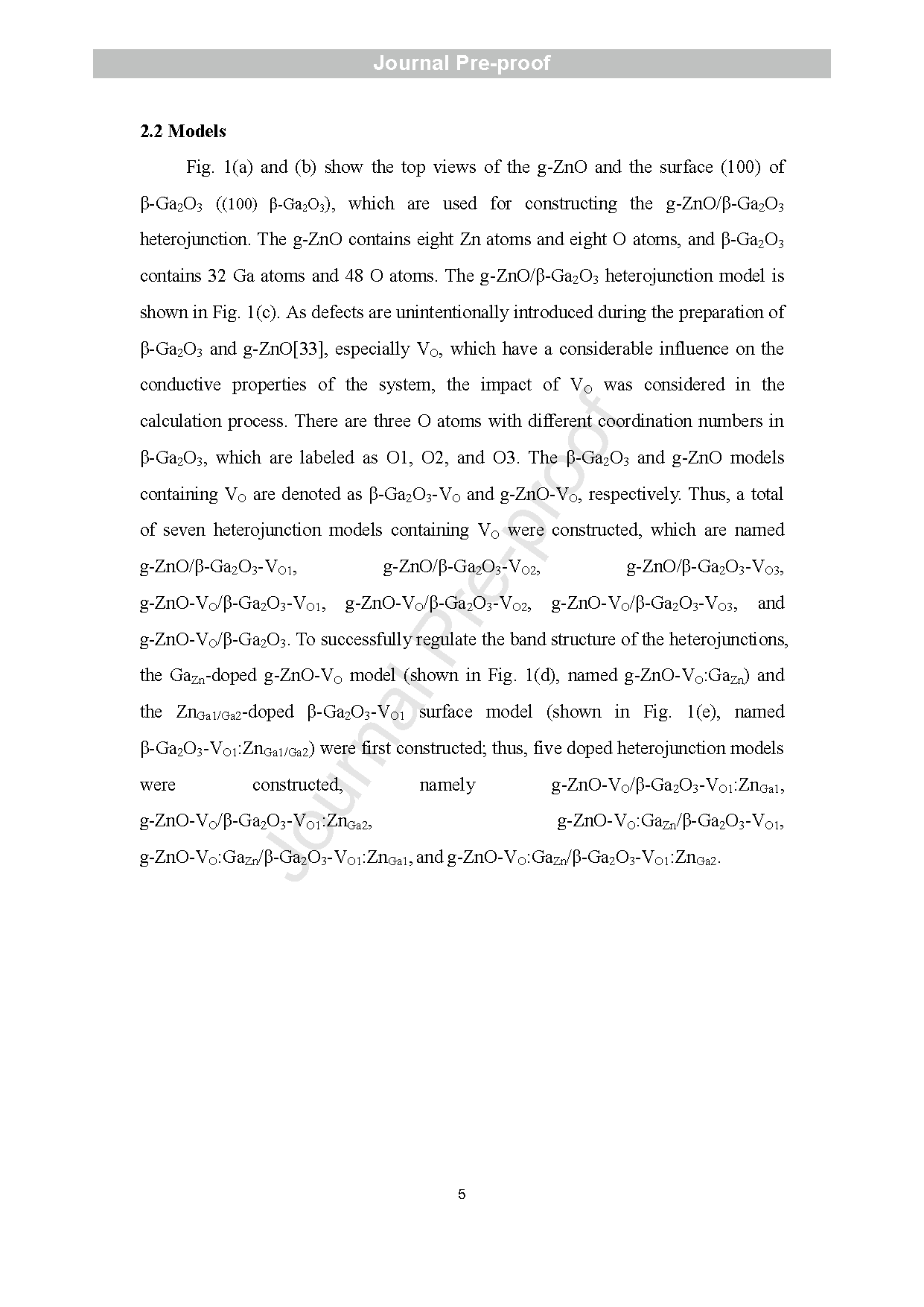
Fig. 1 Models: (a) g -ZnO, (b) (100) β -Ga2O3, (c) g -ZnO/β -Ga2O3 heterojunction, (d) GaZn-doped g-ZnO containing VO, (e) ZnGa-doped (100) β-Ga2O3 containing VO.
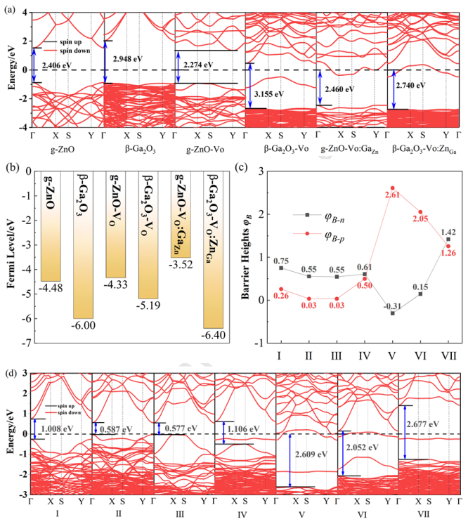
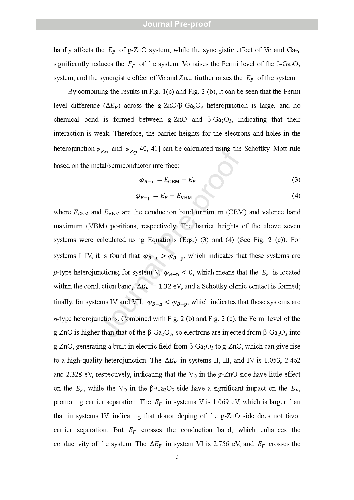
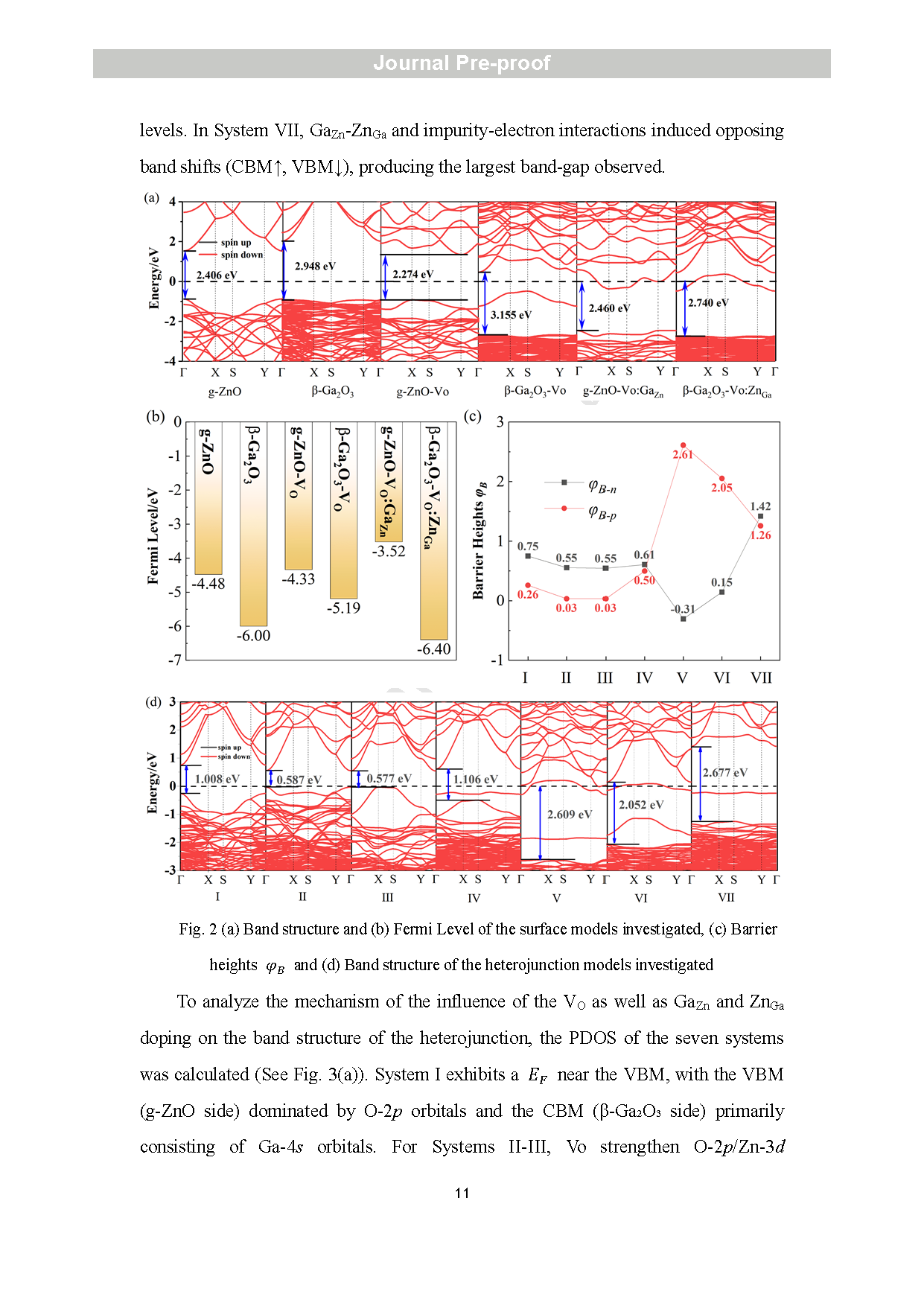
Fig. 2 (a) Band structure and (b) Fermi Level of the surface models investigated, (c) Barrier heights φB and (d) Band structure of the heterojunction models investigated
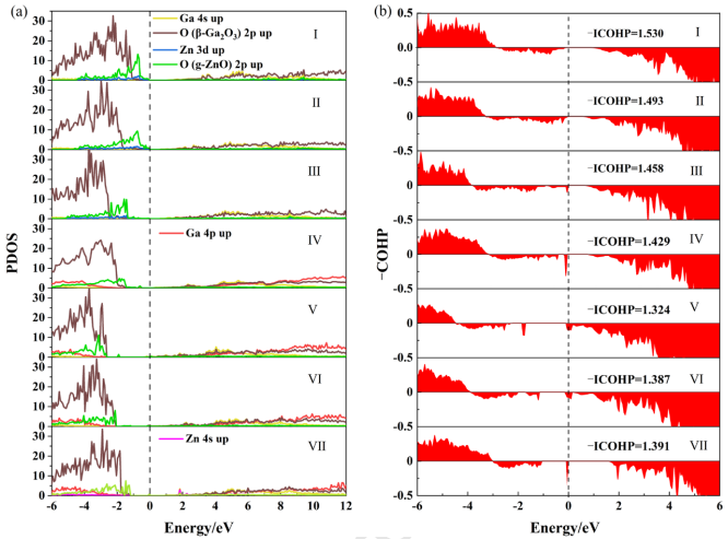
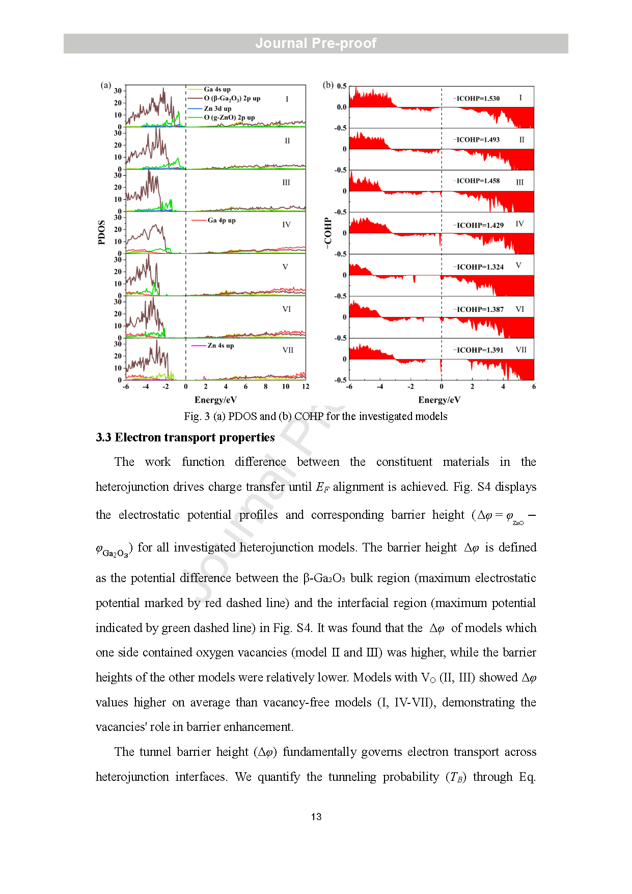
Fig. 3 (a) PDOS and (b) COHP for the investigated models
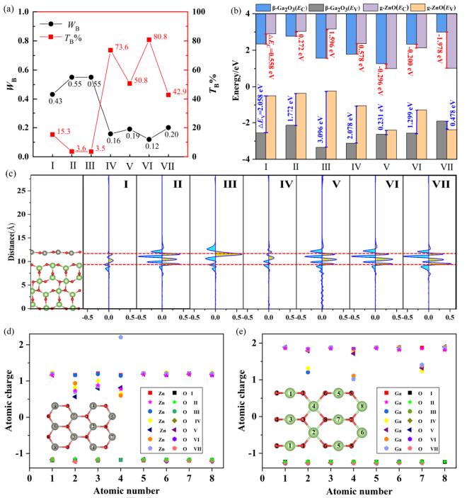
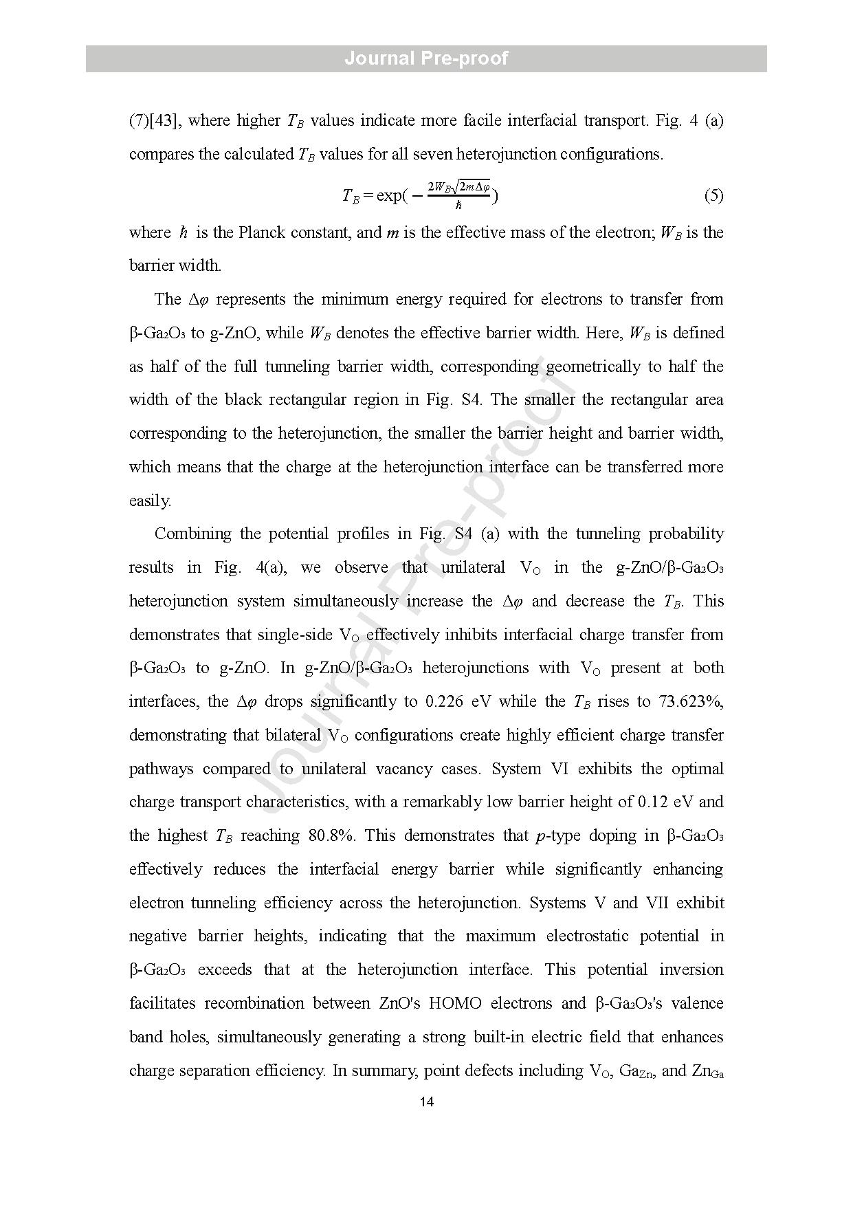
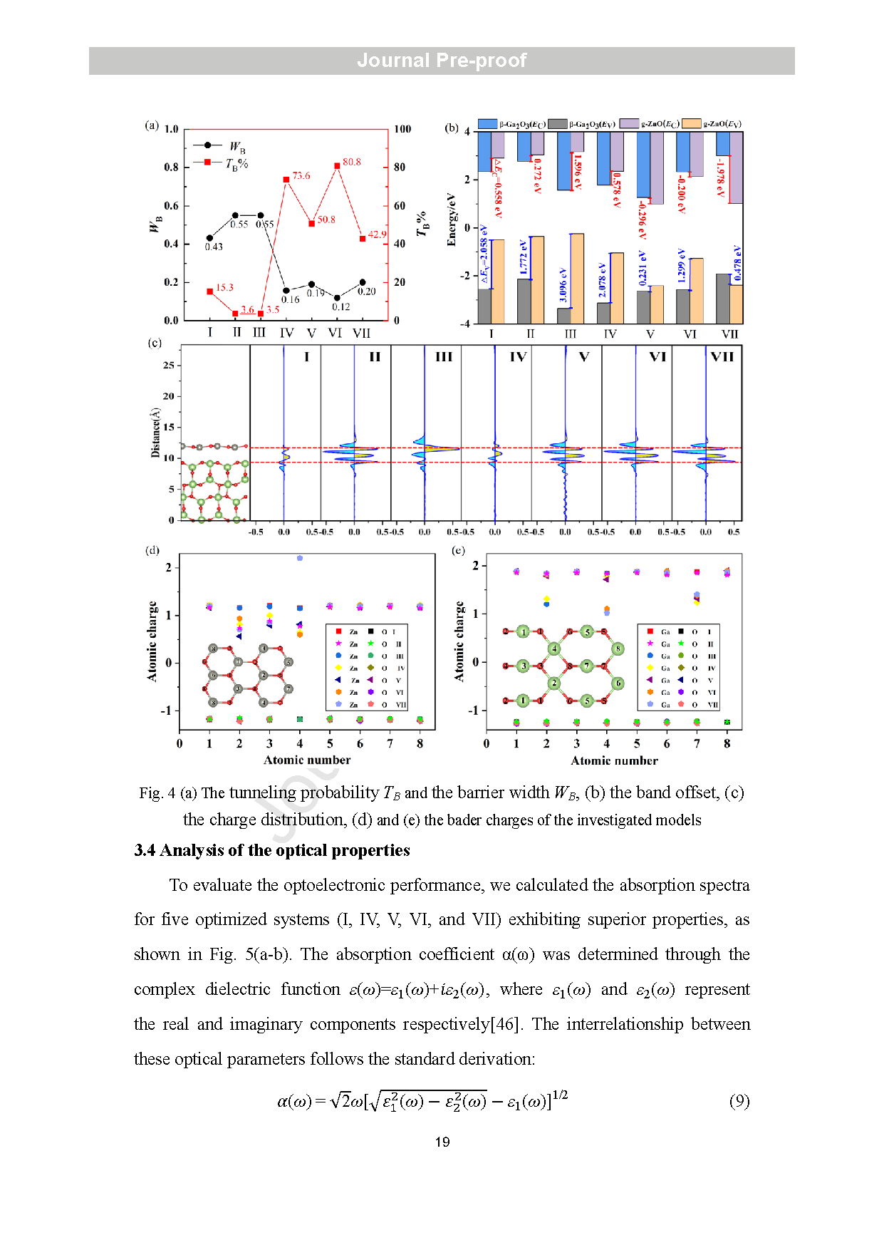
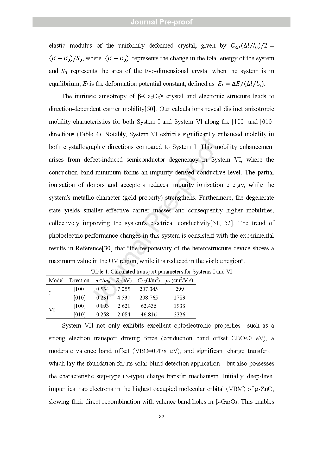
Fig. 4 (a) The tunneling probability TB and the barrier width WB, (b) the band offset, (c) the charge distribution , (d) and (e) the bader charge s of the investigated models
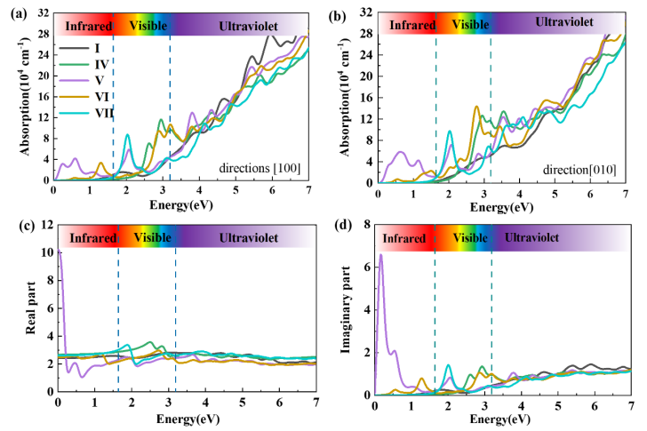
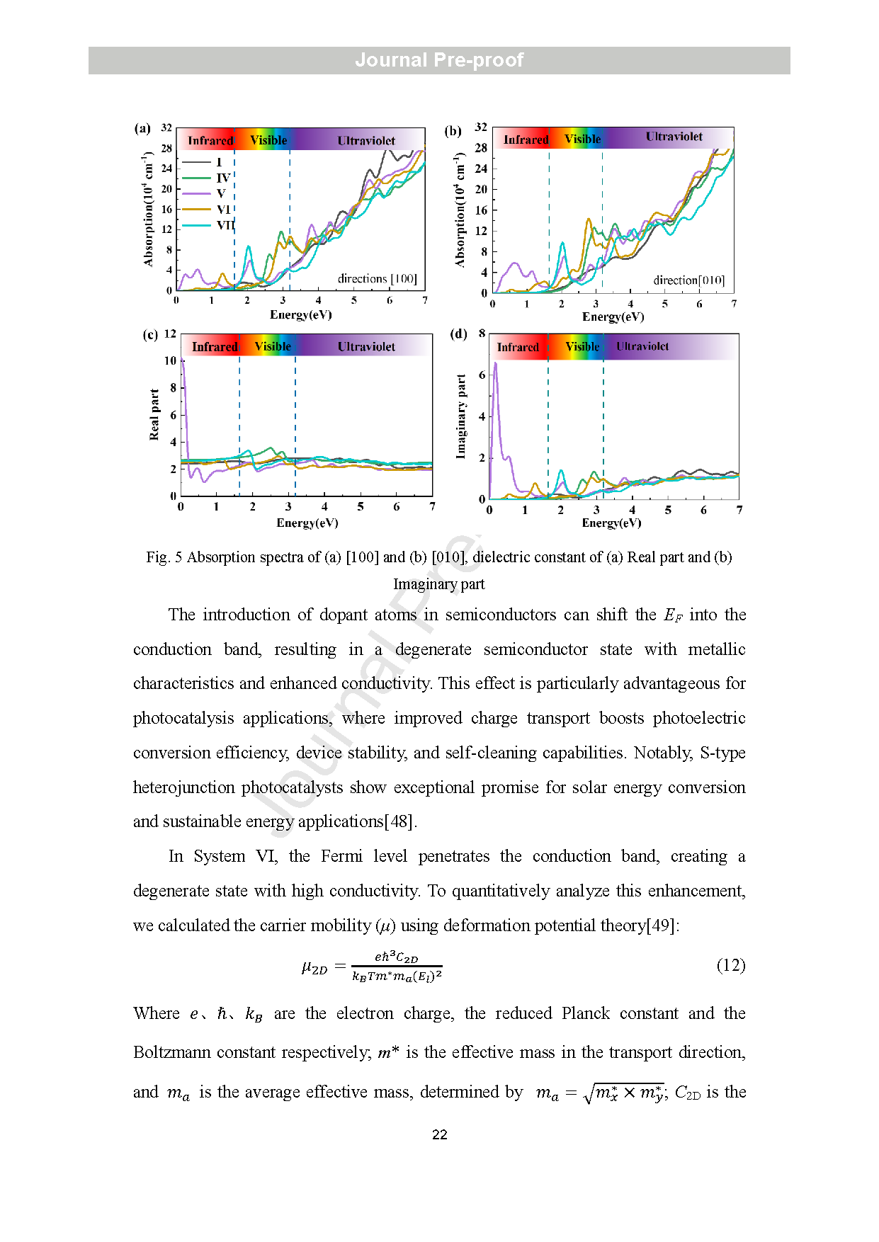
Fig. 5 Absorption spectra of (a) [100] and (b) [010], dielectric constant of (a) Real part and (b) Imaginary part
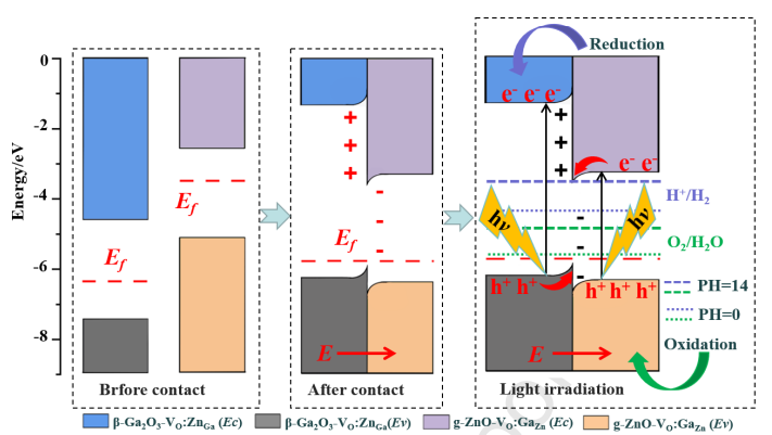
Fig 6 Charge transfer processes in g-ZnO-VO:GaZn/β-Ga2O3-VO1:ZnGa2 heterojunction
DOI:
doi.org/10.1016/j.cej.2025.168841