Paper Sharing
【Member Papers】Toughening beta-Ga₂O₃ via mechanically seeded dislocations
日期:2025-10-23阅读:515
Researchers from the Southern University of Science and Technology have published a dissertation titled "Toughening beta-Ga2O3 via mechanically seeded dislocations" in Materials Science.
Project Support
This work was supported by the Shenzhen Science and Technology Program (Grant No. JCYJ20230807093416034), the Open Fund of the Microscopy Science and Technology–Songshan Lake Science City (Grant No. 202401204), the National Natural Science Foundation of China (Grant No. 52371110), and the Guangdong Basic and Applied Basic Research Foundation (Grant No. 2023A1515011510). X. Fang acknowledges support from the European Union (ERC Starting Grant, Project MECERDIS, Grant No. 101076167). The views and opinions expressed are those of the authors only and do not necessarily reflect those of the European Union or the European Research Council; neither the European Union nor the granting authority can be held responsible for them. G. Zeng acknowledges financial support from the Shenzhen Key Laboratory of Intelligent Robotics Flexible and Manufacturing Systems (Grant No. ZDSYS20220527171403009) and the Shenzhen Science and Technology Innovation Commission (Grant No. 20231115111658002). The authors also acknowledge the use of facilities at the Southern University of Science and Technology Core Research Facility.
Abstract
β-Ga2O3 is a promising candidate for next-generation semiconductors, but is limited by its intrinsic brittleness which hinders its application in flexible electronics and high-precision devices. This study explores a new approach to improving the damage tolerance of (001)-oriented β-Ga2O3 by introducing mechanically seeded dislocations via surface scratching. By applying a Brinell indenter to scratch the surface along the [100] direction, we effectively generate edge-type dislocations belonging to the (011)[01-1] and/or (0-11)[011] slip systems within a mesoscale a wear track. Through a combination of nanoindentation tests, surface morphology analysis, and microstructural characterization using scanning electron microscopy (SEM) and transmission electron microscopy (TEM), we reveal that the introduction of dislocations significantly mitigates the formation of cleavage cracks during indentation, in contrast to that observed in as-received β-Ga2O3. The mechanically seeded dislocations in the subsurface layers play an important role in preventing brittle fracture by facilitating stable plastic deformation.
Conclusion
We demonstrate a novel approach to enhance the damage tolerance and mechanical properties of (001)- oriented β-Ga2O3 through the introduction of mechanically seeded dislocations via surface scratching with a Brinell indenter. Detailed TEM characterization reveals that the scratching-seeded dislocations are edge-type dislocations in the (011)[01-1] and/or (0-11)[011] slip systems. These dislocations effectively suppressed microcrack formation during subsequent nanoindentation testing. Simultaneously, nanoindentation also revealed that the scratched β-Ga2O3 exhibited much higher nano hardness compared to the as-received material. The absence of typical "pop-in" events in the load displacement curves of the scratched samples further corroborates the stabilization of plastic deformation, facilitated by the seeded dislocations. These findings underline the critical role of dislocation engineering in mitigating brittle fracture and enhancing the overall mechanical performance of β-Ga2O3.
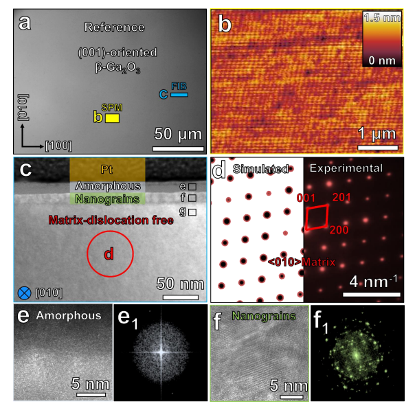
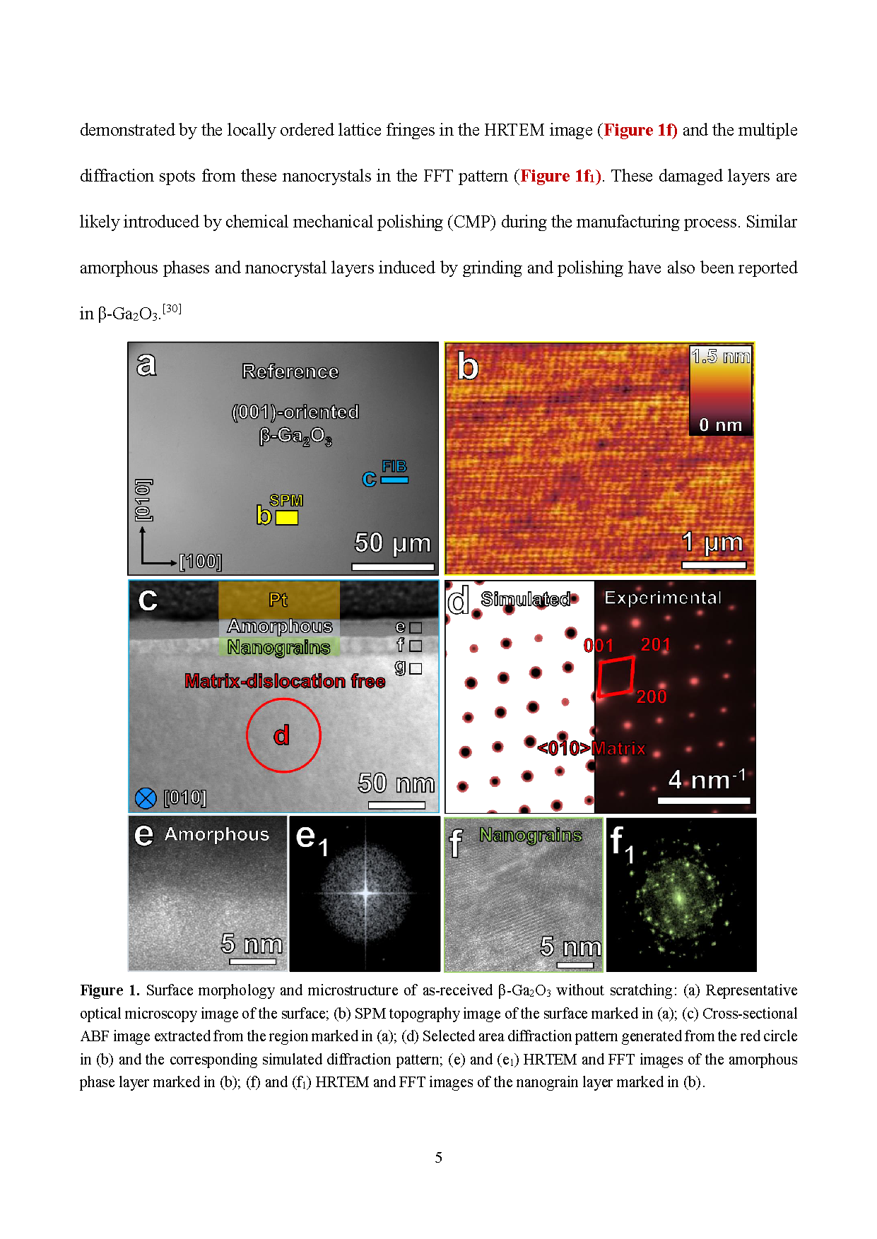
Figure 1. Surface morphology and microstructure of as-received β-Ga2O3 without scratching: (a) Representative optical microscopy image of the surface; (b) SPM topography image of the surface marked in (a); (c) Cross-sectional ABF image extracted from the region marked in (a); (d) Selected area diffraction pattern generated from the red circle in (b) and the corresponding simulated diffraction pattern; (e) and (e1) HRTEM and FFT images of the amorphous phase layer marked in (b); (f) and (f1) HRTEM and FFT images of the nanograin layer marked in (b).
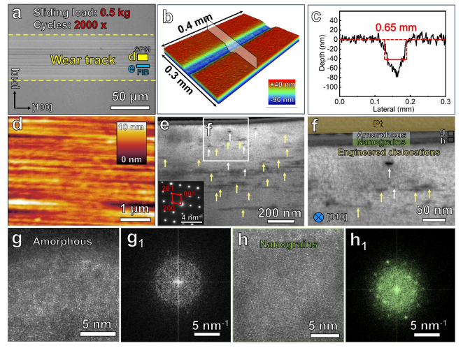
Figure 2. Surface morphology and microstructure of (001)-oriented β-Ga2O3 after scratching: (a) Representative optical microscopy image of the wear track; (b) 3D surface topography image of the wear track measured by white light interferometry; (c) 2D cross-sectional depth profile corresponding to the position marked by the inserted plane in (b); (d) SPM topography image of the wear track in the region marked in (a); (e) Cross-sectional ABF image extracted from the region marked in (a) (the insert shows the corresponding selected area diffraction pattern); (f) Magnified ABF image of the region marked in (e); (g) and (g1) HRTEM and FFT images of the amorphous phase layer marked in (f); (h) and (h1) HRTEM and FFT images of the nanograin layer marked in (f).
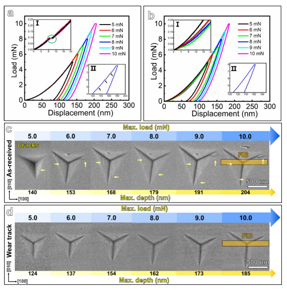
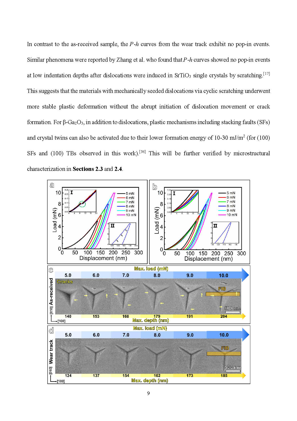
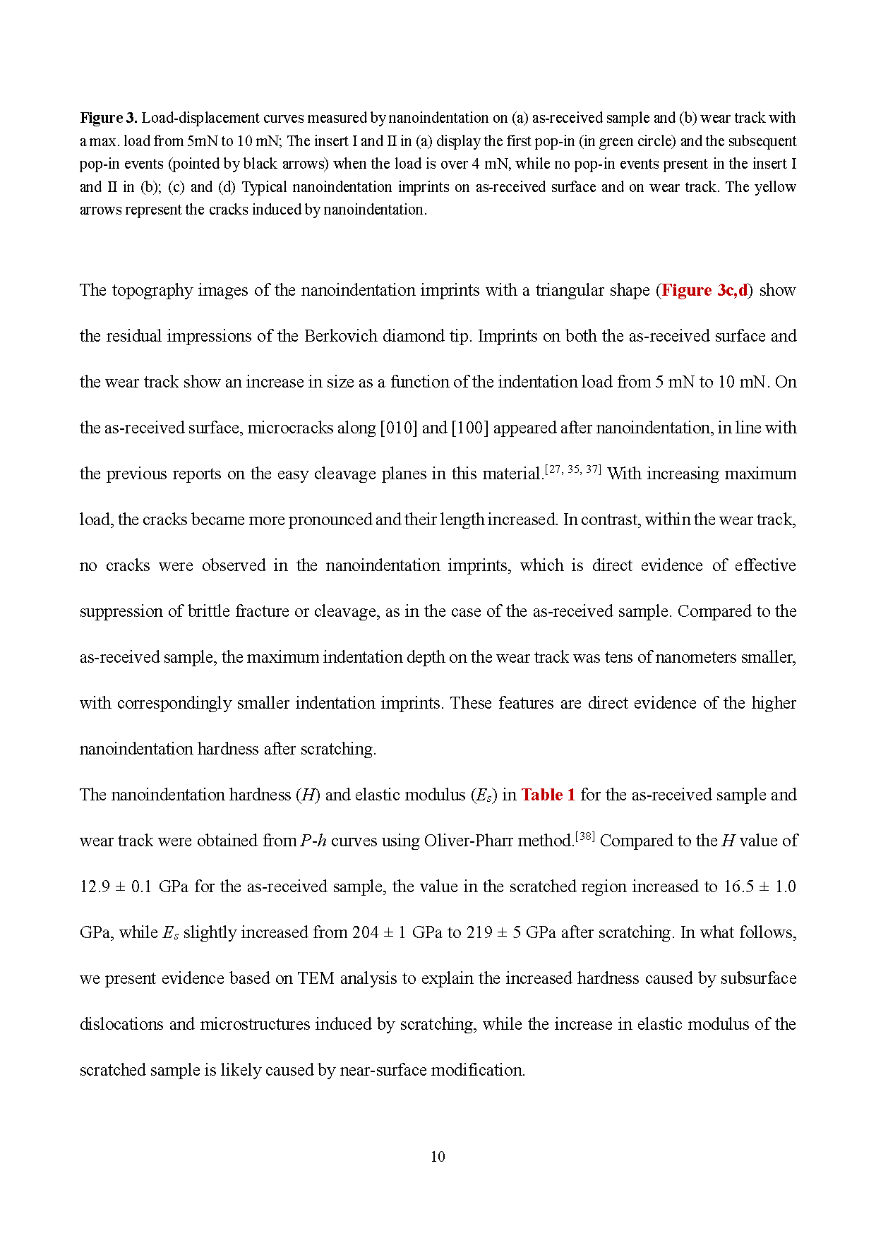
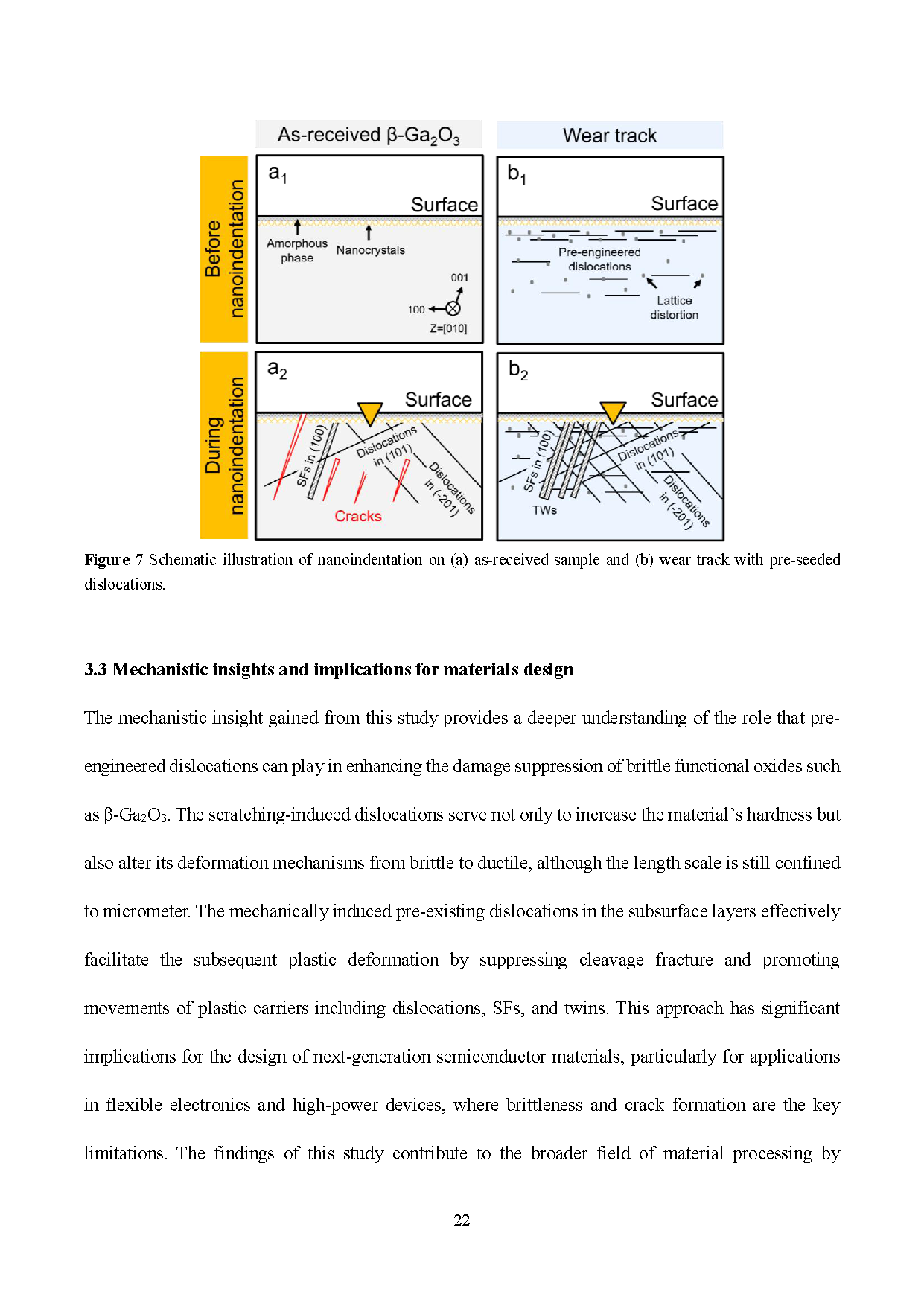
Figure 3. Load-displacement curves measured by nanoindentation on (a) as-received sample and (b) wear track with a max. load from 5mN to 10 mN; The insert Ⅰ and Ⅱ in (a) display the first pop-in (in green circle) and the subsequent pop-in events (pointed by black arrows) when the load is over 4 mN, while no pop-in events present in the insert Ⅰ and Ⅱ in (b); (c) and (d) Typical nanoindentation imprints on as-received surface and on wear track. The yellow arrows represent the cracks induced by nanoindentation.
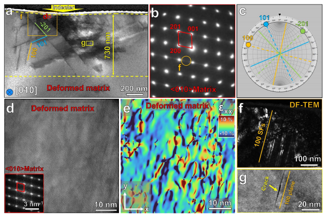
Figure 4. Cross-sectional TEM images of as-received sample after nanoindentation with a max. load of 10 mN: (a) ABF image showing the overview beneath the nanoindentation imprint; (b) Diffraction pattern of the matrix; (c) Stereographic projection analysis representing the slip traces and pole of planes; (d) HRTEM image of the region marked in (a); (e) GPA strain map corresponding to (d); (f) Dark-field image taken by the diffraction streaks marked by the circle in (b); (g) Magnified annular dark field (ADF) image of a crack along (100) plane in (a).
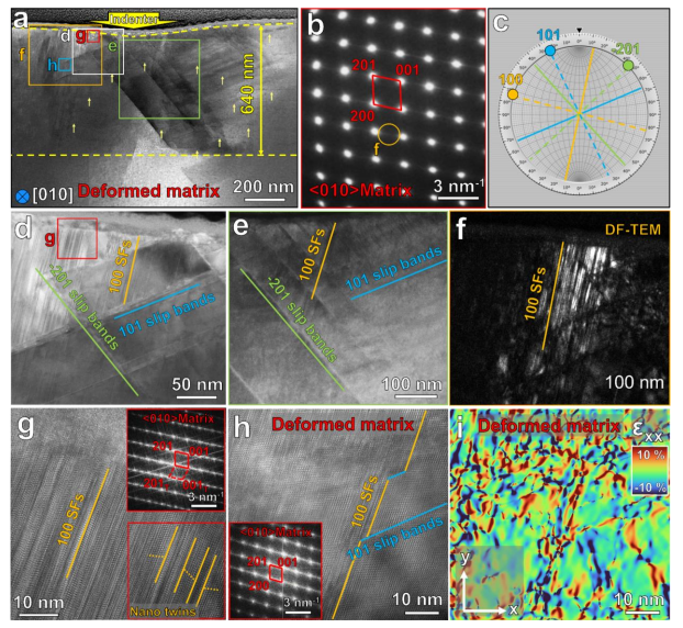
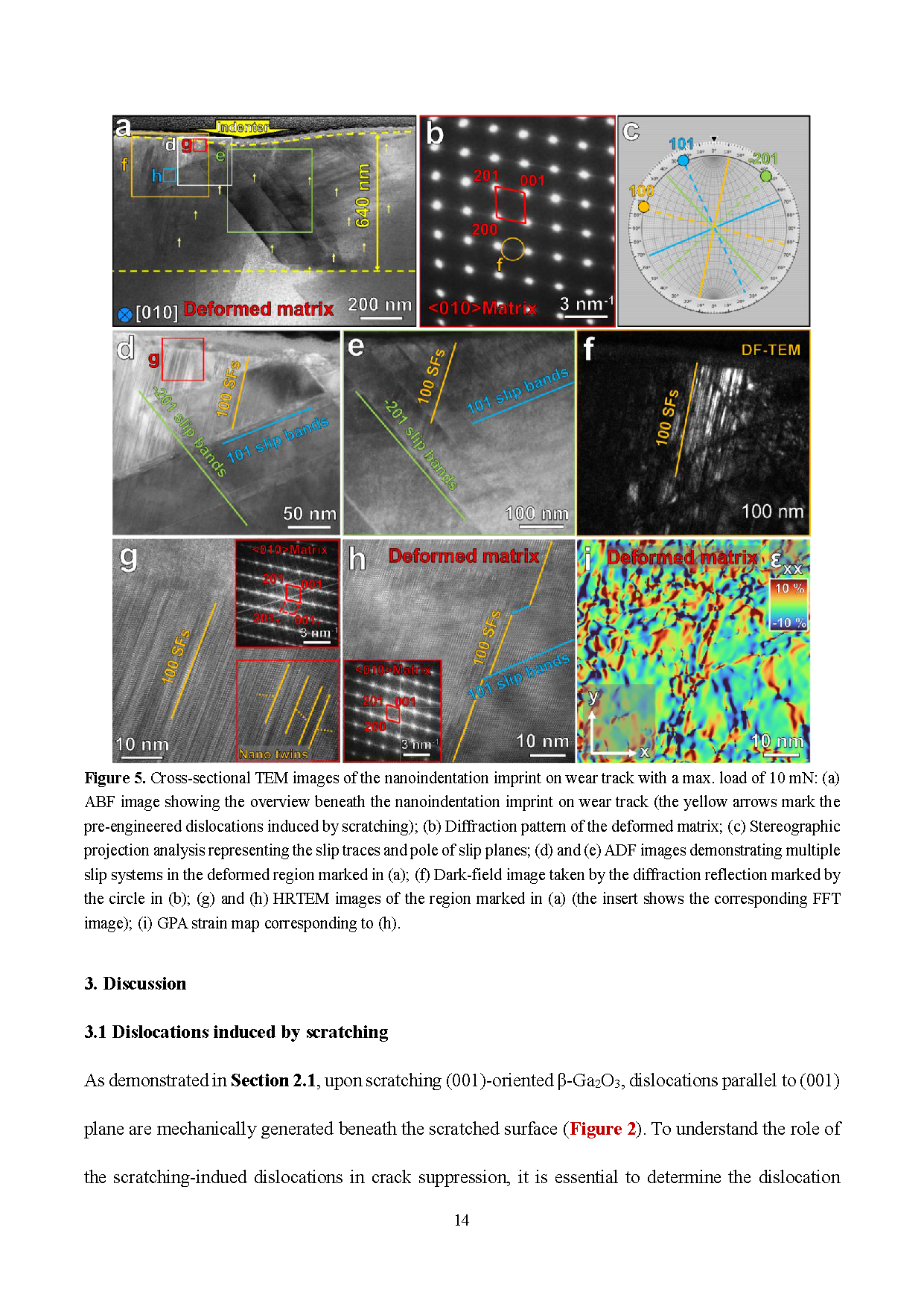
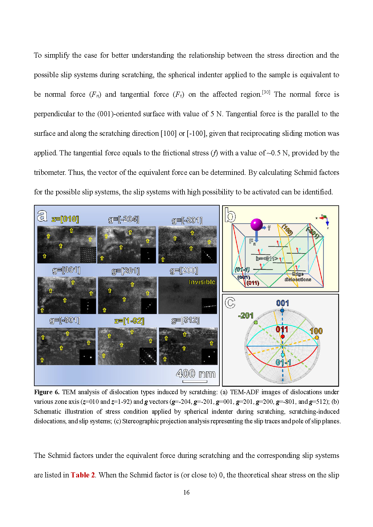
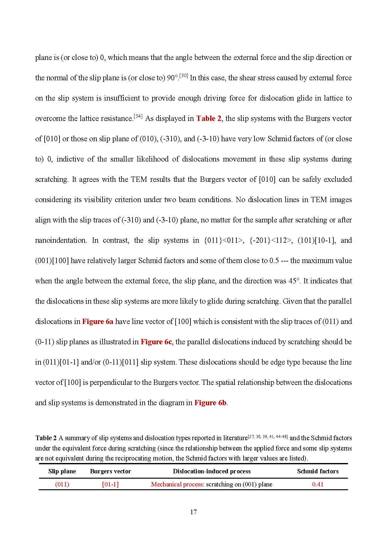
Figure 5. Cross-sectional TEM images of the nanoindentation imprint on wear track with a max. load of 10 mN: (a) ABF image showing the overview beneath the nanoindentation imprint on wear track (the yellow arrows mark the pre-engineered dislocations induced by scratching); (b) Diffraction pattern of the deformed matrix; (c) Stereographic projection analysis representing the slip traces and pole of slip planes; (d) and (e) ADF images demonstrating multiple slip systems in the deformed region marked in (a); (f) Dark-field image taken by the diffraction reflection marked by the circle in (b); (g) and (h) HRTEM images of the region marked in (a) (the insert shows the corresponding FFT image); (i) GPA strain map corresponding to (h).
DOI:
doi.org/10.48550/arXiv.2508.20439