Paper Sharing
【Member Papers】Atomic-scale in situ TEM investigation of electron beam-induced repair of multiple defects in α-Ga₂O₃ heterogeneous epitaxial single-crystal films
日期:2025-11-03阅读:564
Researchers from the Xidian University have published a dissertation titled "Atomic-scale in situ TEM investigation of electron beam-induced repair of multiple defects in α-Ga2O3 heterogeneous epitaxial single-crystal films" in Applied Physics Letters.
Project Support
This study was supported by the National Natural Science Foundation of China (Grant Nos. 62274130, 62188102, 62204185, and 62574157), the Natural Science Basic Research Program of Shaanxi (Program No. 2024JC-YBMS-310), the Fund from Department of Science and Technology in Shaanxi Province (Grant No.2016FWPT09), the China Postdoctoral Science Foundation (Certificate No. 2024T170693), the Tian Chi Ying Cai Project of Xinjiang Uygur Autonomous Region, and the Fundamental Research Funds for the Central Universities and the Innovation Fund of Xidian University. The authors thank the Instrumental Analysis Center of Xidian University for the technical support and also gratefully thank Dr. Xiubo Yang at the Analytical & Testing Center of Northwestern Polytechnical University for assistance with the TEM characterization.
Background
a-Ga2O3, as a phase in the allotropic system of Ga2O3, has become another new research hotspot in the semiconductor field due to its high Baliga’s figure-of-merit (BFOM) and its ability to regulate the bandgap width by alloying with other corundum structural oxides. The bandgap width of α-Ga2O3 (5.3 eV), breakdown field strength (10MV/cm), and BFOM are all higher than those of β-Ga2O3. It is also theoretically suitable for power electronic devices and solar blind detector applications. Currently, power electronic devices based on α-Ga2O3 have been reported on devices such as Schottky diodes, PN junction diodes, and MOSFETs, and the performance of some devices is even better than that of b-Ga2O3-based devices. In particular, the diodes with only α-Ga2O3 thin film manufactured by stripping transfer technology reported in 2016 have heat dissipation characteristics close to commercial SiC devices. In addition, A.V. Almaev et al. have also manufactured the gas sensor and ultraviolet detector based on α-Ga2O3, which further expands the application range of α-Ga2O3. Moreover, Menghan Li et al. realized the controllable growth of high-quality two-dimensional (2D) α-Ga2O3 on the surface of liquid metal gallium by chemical vapor deposition. Several research calculations show that 2D α-Ga2O3 exhibits strain-tunable electronic properties, carrier mobility, and optical absorption, providing direction for the application of low dimensional electronic and optoelectronic devices.
Abstract
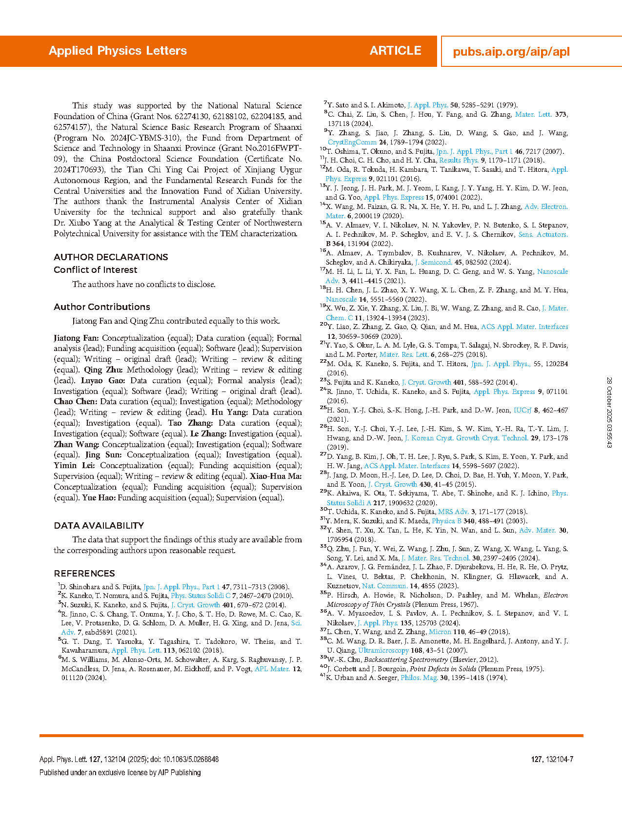
In the process of epitaxial growth of α-Ga2O3, high density dislocations influence the quality of materials and the performance of devices. In this work, the effects of electron beam irradiation in transmission electron microscope (TEM) on different kinds of defects in α-Ga2O3 were studied. For dislocations, in situ dark field images based on different diffraction vectors and high-resolution TEM images both indicate that after electron beam irradiation (2500 e/Å2s), the repair phenomenon of dislocations with a Burgers vector of 1/3 ⟨11-23⟩ and 1/3 ⟨1-100⟩ is observed. With respect to larger size defects, the nano pit (8 × 5 nm2)was repaired to a large extent along (10-14) after irradiation by an electron beam of 2500 e/Å2s for 39 min. Under electron beam irradiation with the same intensity for 42 min, the nanopore (10 × 9 nm2) was partially repaired along (0006) due to the more severe damage. This discovery provides a method to reduce the defects in two-dimensional α-Ga2O3, which is conducive to the further understanding of the properties of two-dimensional α-Ga2O3 and the development of a variety of devices based on it. At the same time, the potential impact of electron beam irradiation needs to be considered in the process of device manufacturing and the reliability of devices in space. On the contrary, this work also provides positive guidance for defect repair in other semiconductor materials that may be sensitive to electron beam irradiation.
Conclusion
This work systematically explores the effects of TEM e-beam irradiation on different types and scales of defects in α-Ga2O3. For dislocations, in situ DF images based on different diffraction vectors and HRTEM images both indicate that after electron beam irradiation (2500 e/Å2s), the repair of dislocations with a Burgers vector of 1/3⟨11-23⟩ and 1/3⟨1-100⟩ is observed. On the contrary, for the nano pit with a size of about 8 × 5 nm2, after being irradiated by an e-beam with an intensity of 2500 e/Å2s s for a certain time, the nano pit is basically repaired along (10-14); However, the ability of e-beam irradiation to repair defects is limited. For another nanopore with dimensions of about 10 × 9 nm2, after being irradiated with the same intensity e-beam for a certain time, the nanopore was partially repaired along (0006), but the central part was still a nanopore. At present, the mainstream application of α-Ga2O3 is still semiconductor devices based on epitaxial film, and there is no report of actual semiconductor devices based on 2D α-Ga2O3. However, several studies on theoretical calculations of 2D α-Ga2O3 show that it has strain-tunable electronic properties, carrier mobility, and optical absorption, which makes 2D α-Ga2O3 very suitable for the application of low dimensional electronic and optoelectronic devices. When α-Ga2O3 is applied to 2D structures or devices, its morphology is closer to that of the TEM samples. At this time, e-beam irradiation can play a similar role in reducing defect density and improving material quality. At the same time, e-beam irradiation has become an important factor to consider in the process of device manufacturing and the selection of the device service environment.

FIG. 1. (a) Low-magnification TEM image of the cross section of α-Ga2O3 epitaxial single-crystal film; (b) enlarged image of α-Ga2O3 epitaxial single-crystal film; (c) SAED image at the α-Ga2O3/α-Al2O3 interface; (d) HRTEM image of α-Ga2O3 film; (e) IFFT image of the yellow dashed box area in (d); and (f) profile strength plot at the blue box in (e).

FIG. 2. (a) Low magnification BF images; (b) SAED of initial sample. (d)–(g) BF images; DF images formed by (h)–(k) g→ = 3-300; and (l)–(o) g→ = 0006 of the sample at different e-beam irradiation time.

FIG. 3. (a) and (b) HRTEM images; (c-f) IFFT images based on 10-10 and 0006 reflections of region I and (g)–(j) IFFT images based on 10-10 and 0006 reflections of region II before and after e-beam irradiation.

FIG. 4. (a)–(d) The repair process of the nano pit under e-beam irradiation (2500 e/A˚2s); (e)–(h) The repair process of the nanopore under e-beam irradiation (2500 e/A˚2s).
FIG. 5. (a) Cs-corrected HRTEM image of α-Ga2O3; (b) STEM-HAADF image; (c) an enlarged image of the square area in (b); and (d)–(I) change in sample morphology at different times.
DOI:
doi.org/10.1063/5.0268848