Paper Sharing
【Member Papers】Recent advancement and perspective of epitaxial growth and doping of β-Ga₂O₃ thin films for power electronics
日期:2025-11-05阅读:609
Researchers from the Xiamen University and Hangzhou Institute of Optics and Fine Mechanics have published a dissertation titled "Recent advancement and perspective of epitaxial growth and doping of β-Ga2O3 thin films for power electronics" in APL Materials.
Project Support
The authors acknowledge the funding support from the National Key R&D Program of China (Grant No. 2022YFB3605501), the Shenzhen Science and Technology Innovation Committee (Grant No. JCYJ20220530143016036), and the National Natural Science Foundation of China (Grant No. 22275154).
Background
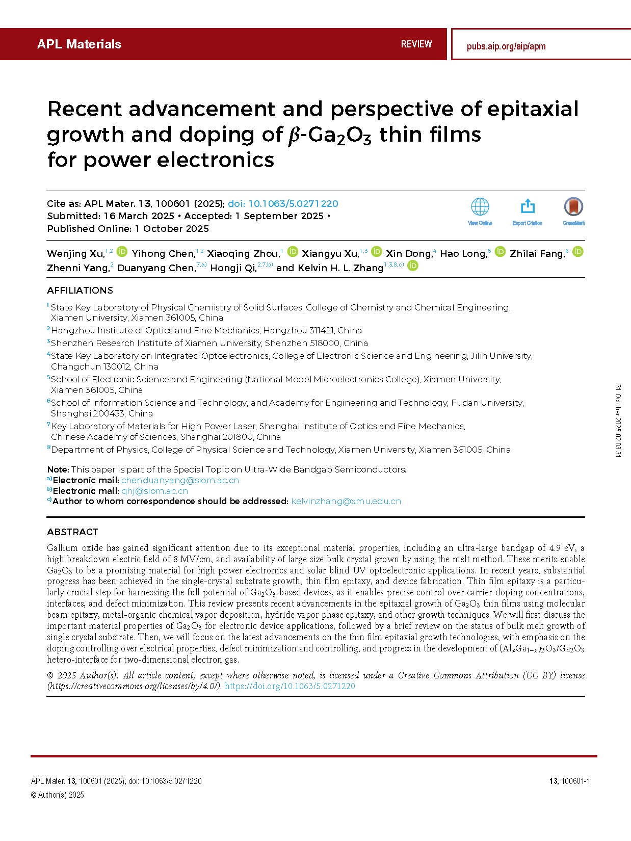
Wide bandgap (WBG) semiconductors, such as silicon carbide (SiC) and gallium nitride (GaN), have garnered significant attention from academia and the semiconductor industry due to their superior material properties, enabling power devices to operate at higher temperatures, voltages, and switching speeds compared to conventional Si-based devices. SiC is particularly well-suited for applications in electric vehicles and power grids, while GaN has gained traction in high-frequency power conversion and fast-charging applications.1 Beyond SiC and GaN, ultra-wide bandgap (UWBG) semiconductors—including gallium oxide (Ga2O3), aluminum nitride (AlN), and diamond—are also receiving growing interest due to their even larger bandgaps (Eg) and superior material properties. Among those intriguing UWBG semiconductors, the emerging monoclinic β-phase Ga2O3 is now regarded as one of the most promising ones for next-generation high-power and high-efficiency electronics, owing to its superior properties and potential for low-cost, large-scale production. The most prominent feature of Ga2O3 is its ultra-large bandgap of ∼4.9 eV, which provides a high electric breakdown field of up to 8 MV/cm due to an exponential relationship between breakdown field and bandgap value (Eg), εc = a(Eg)n, (n = 2–2.5).
Abstract
Gallium oxide has gained significant attention due to its exceptional material properties, including an ultra-large bandgap of 4.9 eV, a high breakdown electric field of 8 MV/cm, and availability of large size bulk crystal grown by using the melt method. These merits enable Ga2O3 to be a promising material for high power electronics and solar blind UV optoelectronic applications. In recent years, substantial progress has been achieved in the single-crystal substrate growth, thin film epitaxy, and device fabrication. Thin film epitaxy is a particularly crucial step for harnessing the full potential of Ga2O3-based devices, as it enables precise control over carrier doping concentrations, interfaces, and defect minimization. This review presents recent advancements in the epitaxial growth of Ga2O3 thin films using molecular beam epitaxy, metal-organic chemical vapor deposition, hydride vapor phase epitaxy, and other growth techniques. We will first discuss the important material properties of Ga2O3 for electronic device applications, followed by a brief review on the status of bulk melt growth of single crystal substrate. Then, we will focus on the latest advancements on the thin film epitaxial growth technologies, with emphasis on the doping controlling over electrical properties, defect minimization and controlling, and progress in the development of (AlxGa1−x)2O3/Ga2O3 hetero-interface for two-dimensional electron gas.
Summary
Owing to the superior material properties of Ga2O3 and the availability of large-size bulk single crystals grown through cost-effective melt-based methods, significant progress has been made in recent years in bulk crystal growth, substrate process, thin film epitaxy, and device fabrication. This article provided a review of the fundamental understanding of Ga2O3 material properties, as well as recent advancements in the synthesis of bulk single crystals, thin-film epitaxy, doping, and defect control.
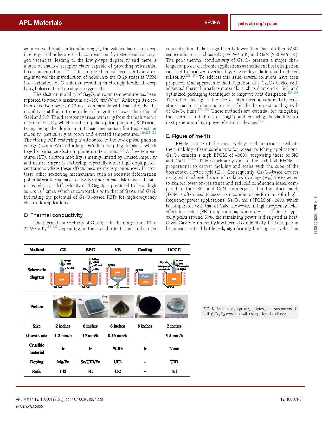
Over the past few years, substantial progress has been achieved in bulk crystal substrate development. The EFG method has enabled the production of large-diameter β-Ga2O3 wafers up to 6 in., with dislocation densities as low as 104 cm−2. In addition, other growth methods such as CZ, VB, and casting have been increasingly explored. For instance, 8 in. bulk crystals have been synthesized using the casting method, while 6 and 2 in. crystals have been produced using VB and CZ, respectively. The 6 in. substrate and epitaxial wafer are expected to be the standard size for mass production in foundries. To make Ga2O3 competitive with SiC, it is crucial to further reduce substrate costs, ideally achieving a 6 in. substrate for $400. Moreover, defect densities in substrates remain relatively high, necessitating further fundamental studies and the development of non-destructive defect inspection techniques.
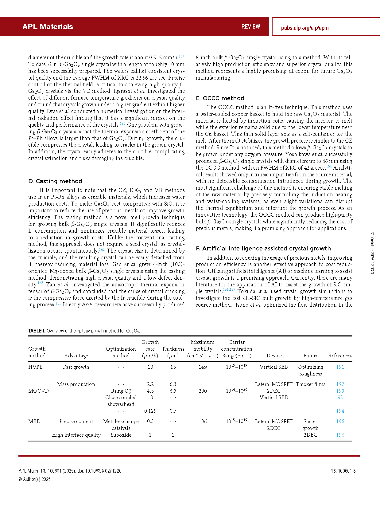
Significant progress has also been made in the epitaxial growth of Ga2O3 thin films and the control of electrical properties through doping. HVPE has demonstrated high growth rates for thick Ga2O3 films, with 4 in. wafers featuring film thicknesses of 10–15 μm now being produced and commercialized. However, challenges such as Cl contamination and surface roughness persist, which require CMP to address. In addition, HVPE may face limitations in further cost reduction. As a result, MOCVD is gaining attention for Ga2O3 epitaxy, given its success in the low-cost, high-efficient mass production of GaN. Recent research has demonstrated the growth of high-quality Ga2O3 films on both (010) and (100) substrates, with mobilities of up to 200 cm2/V s and carrier concentrations controllable from 1015 to 1020 cm−3, primarily using Si dopants. However, these films are typically grown on small substrates with thickness of less than 8 μm and relatively low growth rates compared to HVPE. The next step for MOCVD research will be to achieve thicker films (>10 μm) with faster growth rates (>5 μm/h) on larger wafers (>4 in.), enabling cost-effective production for mass manufacturing. In addition, the high density of large-size defects (killer defects) remains a challenge, and further research is needed to address this issue. Continued efforts to reduce defects, particularly twin boundaries, stacking faults, and large particles, will be critical for improving device reliability and performance. Although MBE has a slow growth rate (<1 nm/h), it excels in providing precise atomic-level control over film growth. This capability enables the fabrication of high-quality epitaxial layers with low defect densities, well-defined doping profiles, and sharp interfaces. MBE is particularly well-suited for the fabrication of (AlxGa1−x)2O3/Ga2O3 2DEG systems for radio frequency devices.
Despite these advancements, β-Ga2O3 has two fundamental limitations: the lack of effective p-type doping and poor thermal conductivity. The absence of p-type material with reasonable hole conductivity imposes significant design constraints on β-Ga2O3 device structures. In addition, its low thermal conductivity adversely affects heat dissipation, posing a serious challenge for high-power device applications.
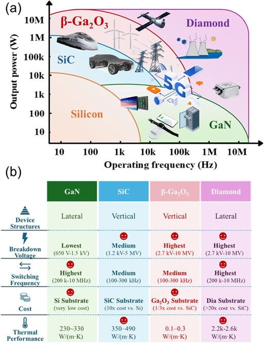
FIG. 1. (a) Bandgap energy vs breakdown field of semiconductors. (b) Applications of SiC, GaN, and Ga2O3 for power electronics in terms of current and voltage requirements.
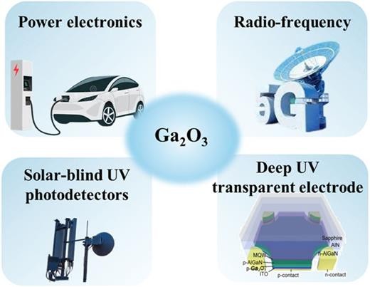
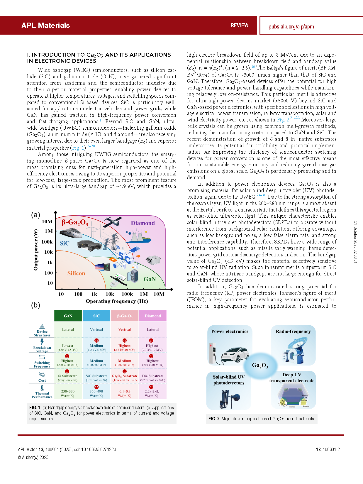
FIG. 2. Major device applications of Ga2O3 based materials.
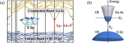
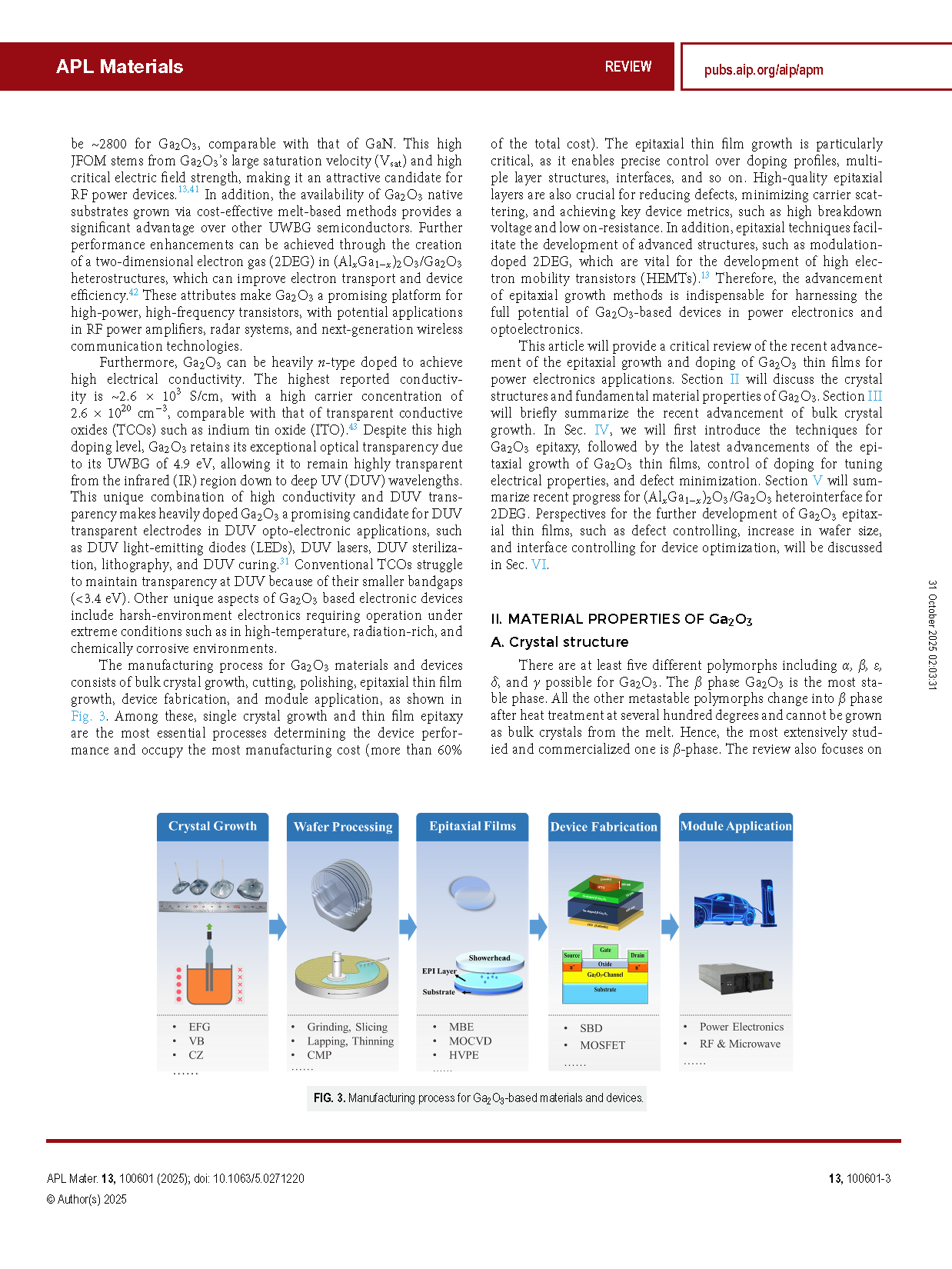
FIG. 3. Manufacturing process for Ga2O3-based materials and devices.
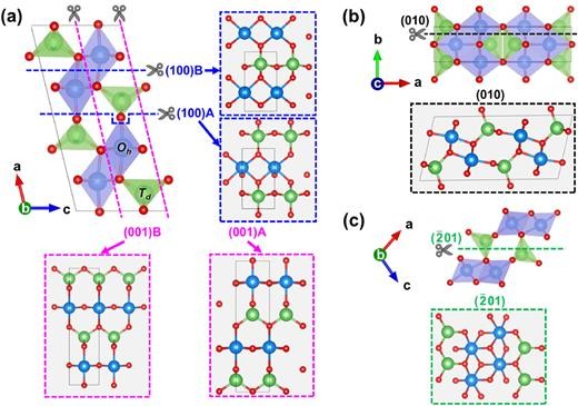
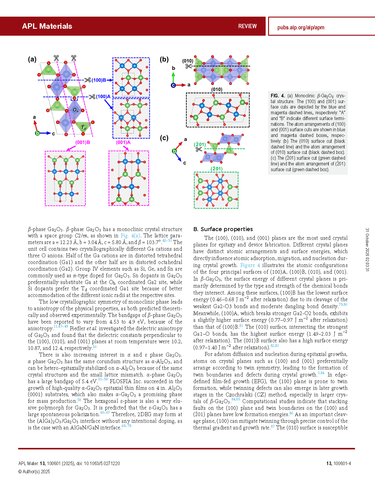
FIG. 4. (a) Monoclinic β-Ga2O3 crystal structure. The (100) and (001) surface cuts are depicted by the blue and magenta dashed lines, respectively. “A” and “B” indicate different surface terminations. The atom arrangements of (100) and (001) surface cuts are shown in blue and magenta dashed boxes, respectively. (b) The (010) surface cut (black dashed line) and the atom arrangement of (010) surface cut (black dashed box). (c) The (-201) surface cut (green dashed line) and the atom arrangement of (-201) surface cut (green dashed box).
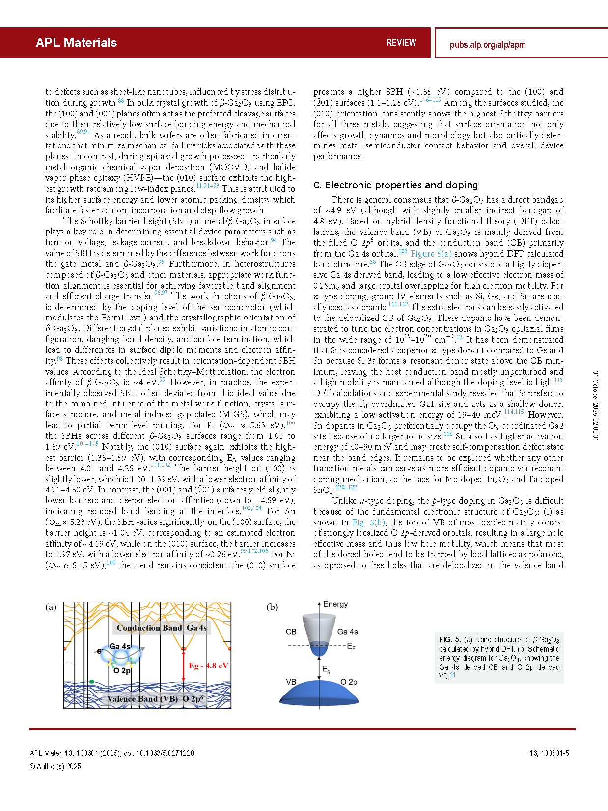
FIG. 5. (a) Band structure of β-Ga2O3 calculated by hybrid DFT. (b) Schematic energy diagram for Ga2O3, showing the Ga 4s derived CB and O 2p derived VB.
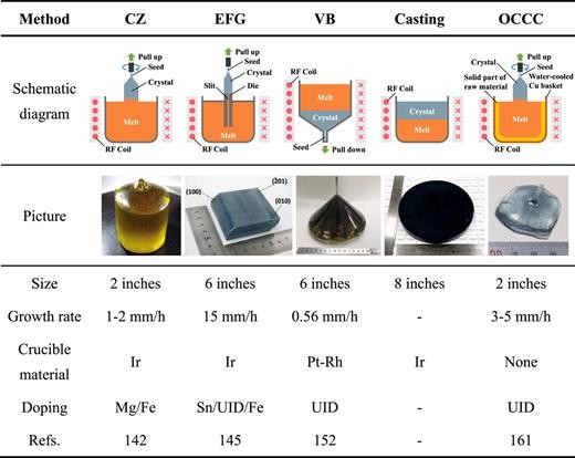
FIG. 6. Schematic diagrams, pictures, and parameters of bulk β-Ga2O3 crystal growth using different methods.
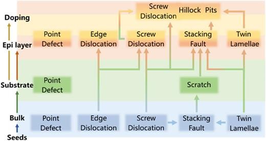
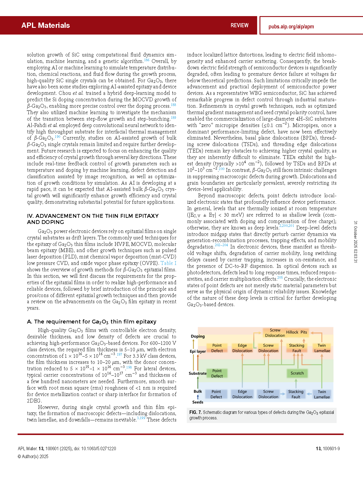
FIG. 7. Schematic diagram for various types of defects during the Ga2O3 epitaxial growth process.
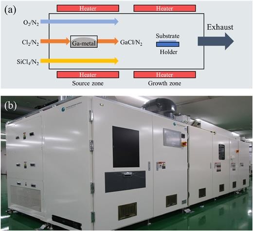
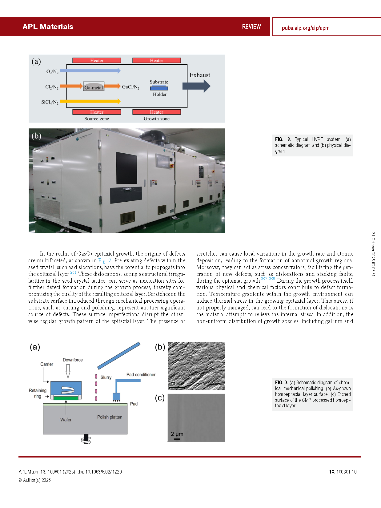
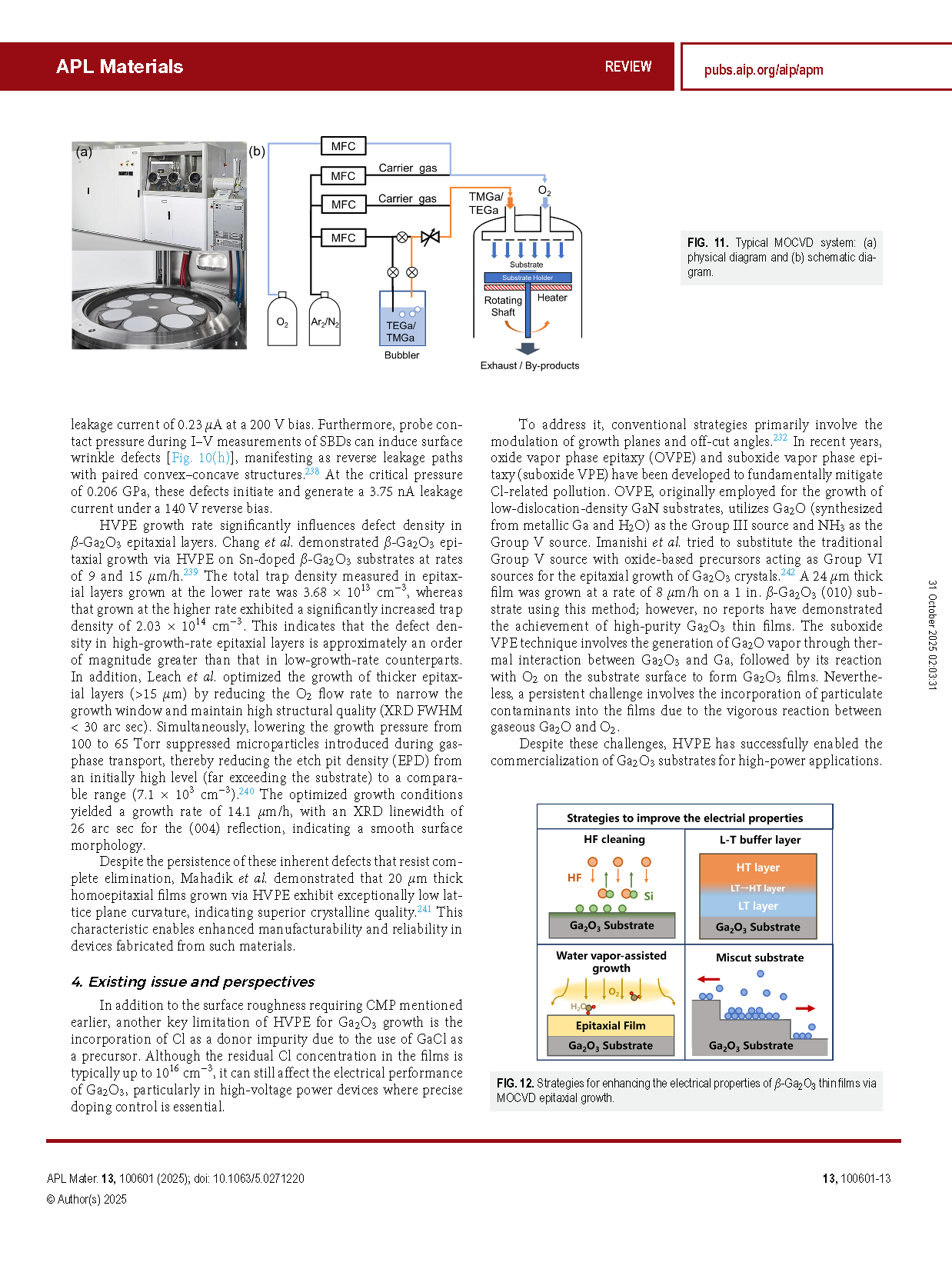
FIG. 8. Typical HVPE system: (a) schematic diagram and (b) physical diagram.
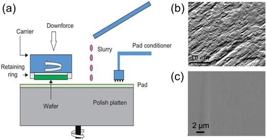
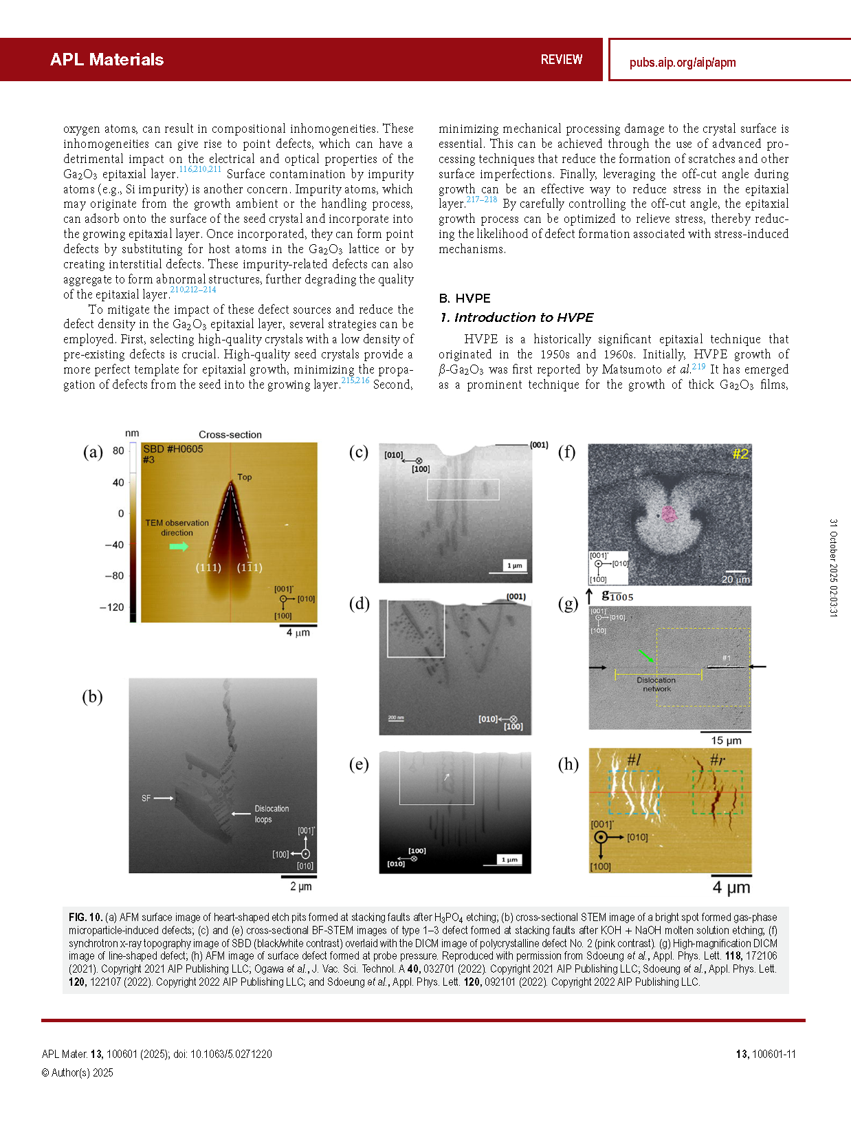
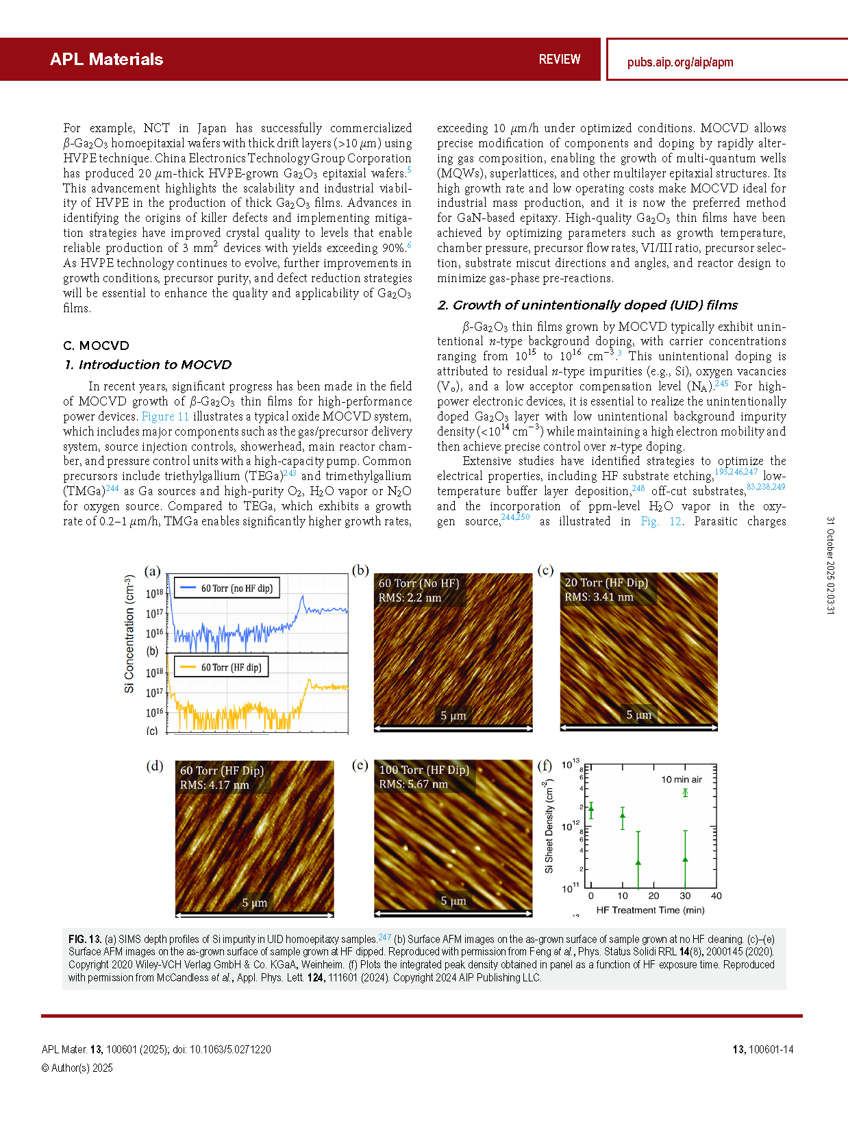
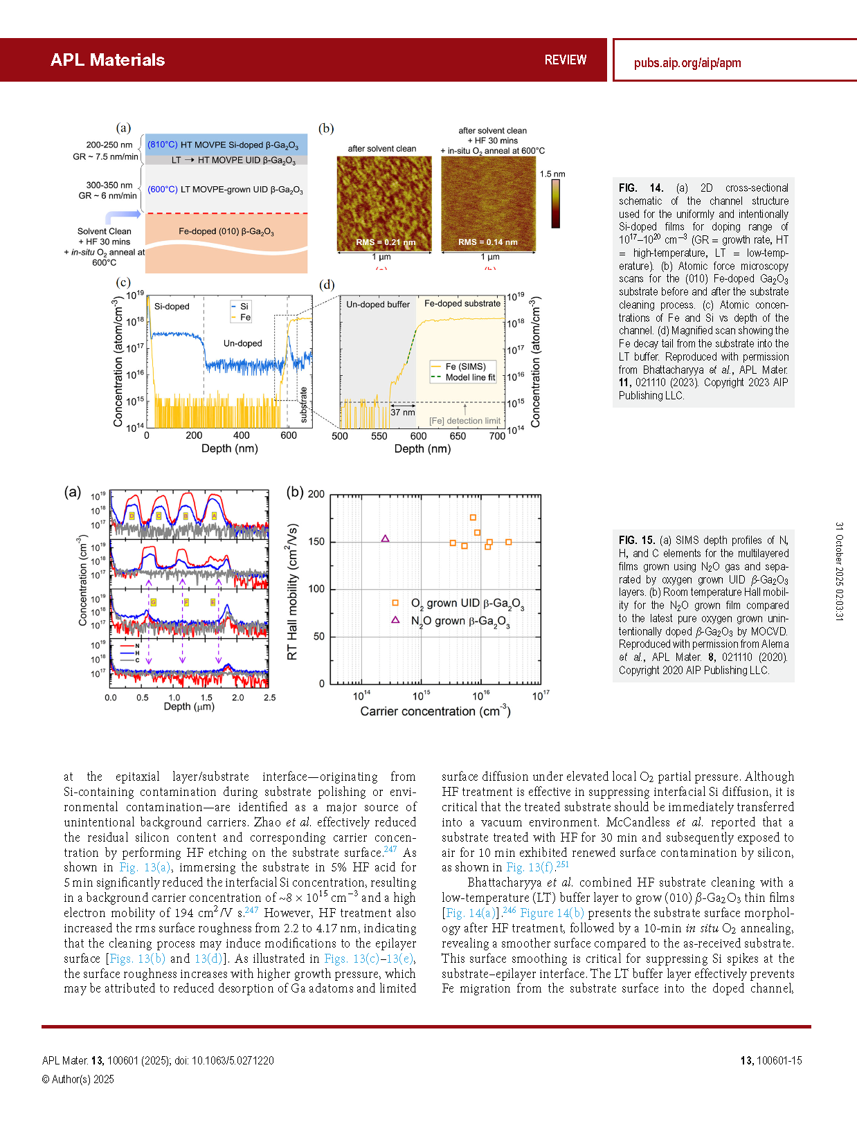
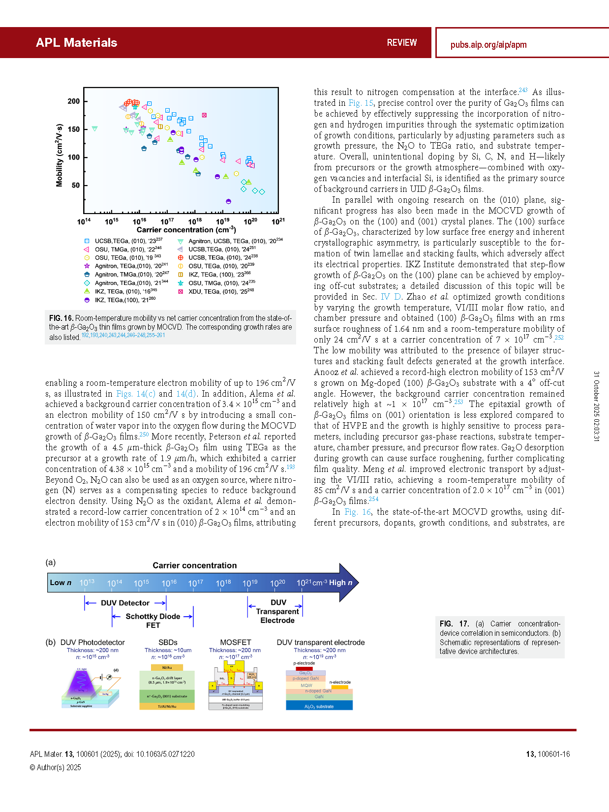
FIG. 9. (a) Schematic diagram of chemical mechanical polishing. (b) As-grown homoepitaxial layer surface. (c) Etched surface of the CMP processed homoepitaxial layer.
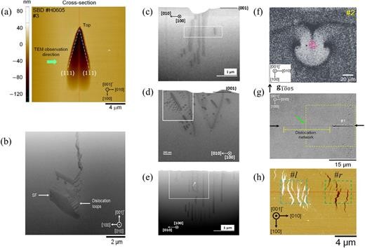
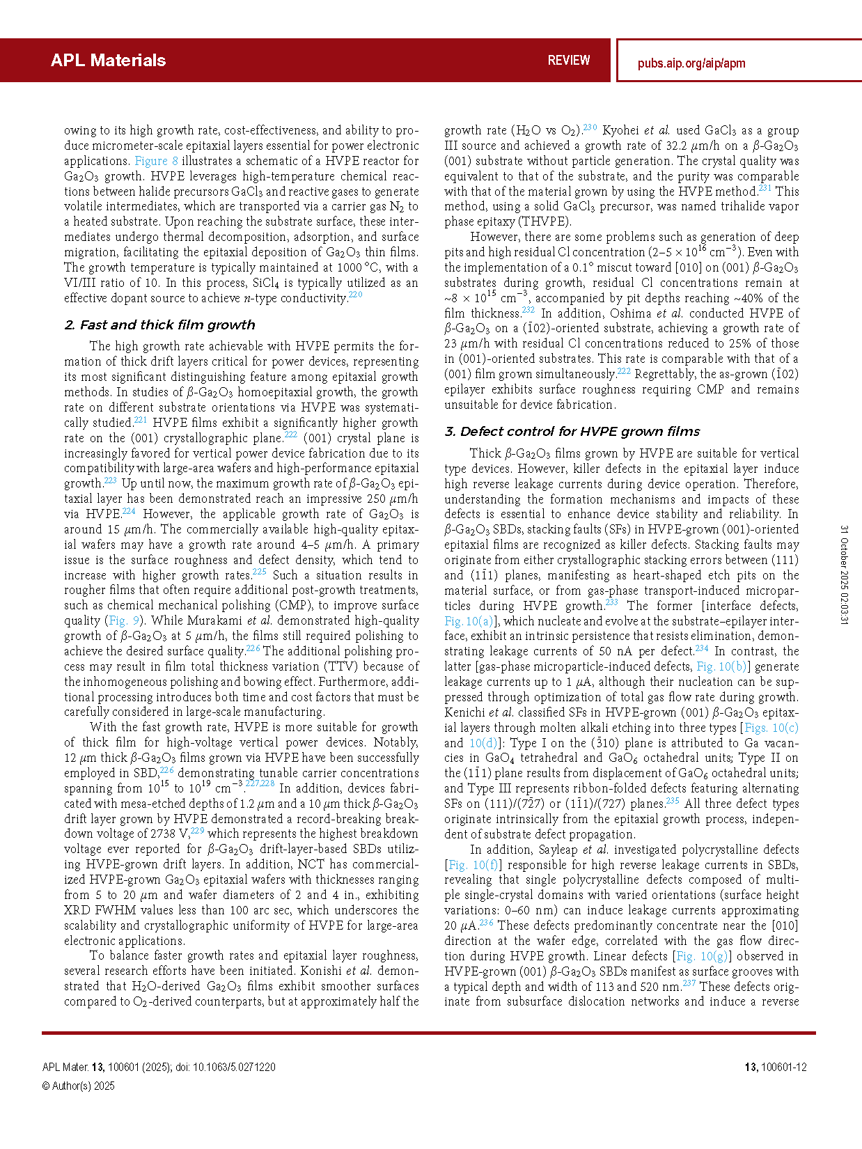
FIG. 10. (a) AFM surface image of heart-shaped etch pits formed at stacking faults after H3PO4 etching; (b) cross-sectional STEM image of a bright spot formed gas-phase microparticle-induced defects; (c) and (e) cross-sectional BF-STEM images of type 1–3 defect formed at stacking faults after KOH + NaOH molten solution etching; (f) synchrotron x-ray topography image of SBD (black/white contrast) overlaid with the DICM image of polycrystalline defect No. 2 (pink contrast). (g) High-magnification DICM image of line-shaped defect; (h) AFM image of surface defect formed at probe pressure. Reproduced with permission from Sdoeung et al., Appl. Phys. Lett. 118, 172106 (2021). Copyright 2021 AIP Publishing LLC; Ogawa et al., J. Vac. Sci. Technol. A 40, 032701 (2022). Copyright 2021 AIP Publishing LLC; Sdoeung et al., Appl. Phys. Lett. 120, 122107 (2022). Copyright 2022 AIP Publishing LLC; and Sdoeung et al., Appl. Phys. Lett. 120, 092101 (2022). Copyright 2022 AIP Publishing LLC.
DOI:
doi.org/10.1063/5.0271220