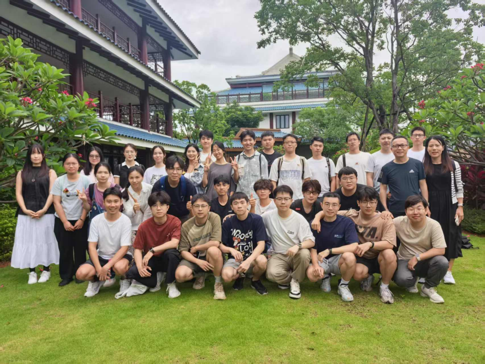

【Specialist Intro】Yang Weifeng —— the Member of Technical Expert Committee
日期:2025-11-07阅读:755

Profile
Yang Weifeng, a professor and Ph.D. supervisor at Xiamen University and the head of the Power Semiconductor laboratory. He is a recipient of the Fujian Province "Minjiang Scholars Award Program", the "Foreign Expert Hundred Talents Program", and the Xiamen City " Double-Hundred Talents Program". His main research areas include epitaxial growth and doping mechanisms of wide bandgap and ultra-wide bandgap semiconductors, device design and simulation, chip manufacturing and module integration. To date, he has published over 100 academic papers in internationally renowned journals and conferences, including Nature Physics, Energy Storage Materials, Applied Physics Letters, IEEE Electron Device Letters, and IEEE Transactions on Electron Devices. He has also applied for more than 20 invention patents, several of which have been successfully industrialized.

Group homepage:
http://team.xmu.edu.cn/XMU_PSL/zh_CN/index.htm
Achievements
1、Research on Gallium Oxide Epitaxial Growth and Devices
Investigating the mechanisms of homoepitaxy and heteroepitaxy of Ga₂O₃ to achieve wafer-scale epitaxial growth. Developed a series of high-performance power devices (SBD/HJ/MOSFET, etc.) and solar-blind ultraviolet photodetectors (MSM/PN/PIN, etc.), including the first photodetector diode and power diode based on a CuCrO₂/Ga₂O₃ p–n junction.
2、Research on High-Power Gallium Nitride HEMT Power Chips
Developed a series of 650 V E-mode GaN HEMT power chips for applications in new energy vehicles and industrial motors, with specifications including 50 mΩ, 25 mΩ, and 10 mΩ. Key performance metrics of these chips have reached world-class standards, with the 10 mΩ chip achieving the lowest on-resistance among commercially available 650 V GaN chips globally.
3、Research on Photovoltaic Inverters Based on Gallium Nitride and Silicon Carbide
Enabled products through circuit improvements and algorithm innovation, developing a series of high-performance circuit modules and photovoltaic inverters based on SiC MOSFETs and GaN HEMTs.
4、Research on Silicon Carbide Ultraviolet Photodetectors and Power Devices
Developed a series of high-performance SiC ultraviolet photodetectors and power devices, including MSM, MISIM, PIN, APD, and JBS structures.
[1] W. F. Yang* et al, Applied Physics Letters 126(15), 152108 (2025).
[2] W. F. Yang* et al, IEEE Electron Device Letters 46(11), 1966-1969 (2025).
[3] W. F. Yang* et al, IEEE Transactions on Electron Devices 72(8), 4005-4010 (2025).
[4] W. F. Yang* et al, IEEE Sensors Journal 25(13), 24096-24105 (2025).
[5] W. F. Yang* et al, IEEE Transactions on Electron Devices, doi: 10.1109/TED.2025.3621417 (2025).
[6] W. F. Yang* et al, IEEE Transactions on Electron Devices 71(5), 3045-3049 (2024).
[7] W. F. Yang* et al, IEEE Sensors Journal 24(9), 14109-14117 (2024).
[8] W. F. Yang* et al, IEEE Transactions on Electron Devices 71(11), 6934–6941 (2024).
[9] W. F. Yang* et al, IEEE Sensors Journal 24(24), 40717–40724 (2024).
[10] W. F. Yang* et al, IEEE Photonics Technology Letters 36(9), 593-596 (2024).
[11] A PN Junction Ga₂O₃-Based MODFET Device and Its Fabrication Method, Patent No.: 202411346806.6
[12] A Ga₂O₃ Schottky Diode with AlN Barrier Layer and Its Fabrication Method, Patent No.: 202311264299.7
[13] Normally-Off Ga₂O₃-Based Device Epitaxially Grown After MBE Etching and Its Fabrication Method, Patent No.: 202310862139.6
[14] A Ga₂O₃-Based MIS-HEMT Device and Its Fabrication Method, Patent No.: 202111021113.6
[15] A Normally-On Ga₂O₃-Based HFET Device with Cap Layer and Its Fabrication Method, Patent No.: 202110974627.7
[16] A Normally-Off Ga₂O₃-Based MIS-HFET Device, Patent No.: 202110493226.X
Expert's Message
As a highly promising next-generation semiconductor material, gallium oxide (Ga₂O₃) has achieved a legendary pace of development in the history of semiconductors—commercial breakthroughs on 6- and 8-inch substrates have been realized within just a few years. However, Ga₂O₃ still faces challenges in key technologies such as thermal management and p-type doping. We look forward to collaborating with industry peers to tackle these challenges together, build a robust Ga₂O₃ ecosystem, and advance both the industry and critical technologies in this field!


