Paper Sharing
【International Papers】Over 3 kV and Ultra-Low leakage Vertical (011) β-Ga₂O₃ Power Diodes with Engineered Schottky Contact and High-permittivity Dielectric Field Plate
日期:2025-11-18阅读:638
Researchers from the Iowa State University have published a dissertation titled " Low leakage Vertical (011) β-Ga2O3 Power Diodes with Engineered Schottky Contact and High-permittivity Dielectric Field Plate ". This work utilized (011) substrates provided by Novel Crystal Technology, Japan.
Background
β-Ga₂O₃ has attracted widespread attention for compact and high-power semiconductor devices due to its ultrawide bandgap (~4.8 eV), controllable shallow dopants, and high critical breakdown field (~8 MV/cm). The availability of melt-grown β-Ga₂O₃ native substrates offers a unique opportunity for cost-effective, large-scale production of ultrawide bandgap (UWBG) power devices. Although various field management techniques—such as field plates, trench structures, guard rings, deep etching, and ion implantation—have been employed to improve the performance of vertical β-Ga₂O₃ power diodes, most reported devices still rely on HVPE-grown ~10 μm-thick (001)-oriented epilayers with relatively high background doping. Moreover, (001) β-Ga₂O₃ epitaxy tends to generate line-shaped dislocations that serve as killer defects, forming leakage paths and degrading breakdown performance, thus limiting voltage scalability. To overcome these issues, homoepitaxial growth of β-Ga₂O₃ in alternative orientations, particularly (011), has been explored since it can reduce dislocation-induced leakage by aligning traps parallel to the (011) plane. However, fundamental studies on the electronic properties and Schottky barrier characteristics of vertical (011) β-Ga₂O₃ Schottky diodes remain limited. Achieving high-voltage operation in such devices requires effective edge field management and engineered Schottky contacts to suppress tunneling leakage and premature breakdown. In this work, vertical (011) β-Ga₂O₃ Schottky barrier diodes were developed by integrating a high-permittivity (ZrO₂) field plate and optimized composite Pt cap/PtOx/Pt (1.5 nm) anode contacts, achieving ultra-low leakage, multi-kilovolt breakdown voltage, and low turn-on voltage—demonstrating the strong potential of (011) β-Ga₂O₃ for next-generation high-voltage power devices.
Abstract
We report (011) β-Ga2O3 power devices with over 3 kV breakdown voltage and ultra-low leakage, achieved through Schottky barrier engineering and high-permittivity (κ) dielectric (ZrO2) field plates. The (011) orientation of β-Ga2O3 enables low background doping and thick drift layers, making it promising for kV-class vertical β-Ga2O3 power switches. Schottky barrier engineering was implemented using a composite Pt cap/PtOx/Pt (1.5 nm) anode contact. This structure takes advantage of the enhanced reverse-blocking capabilities of PtOx while maintaining low turn-on voltage through the thin interfacing Pt layer. A systematic study was conducted on co-processed Pt/(011) β-Ga2O3 Schottky barrier diodes (SBDs) on the same wafer. The bare SBDs exhibited a breakdown voltage of ~1.5 kV, whereas field-plate Pt/(011) β-Ga2O3 SBDs showed an increased breakdown voltage of 2.75 kV due to edge-field management. Further enhancement was achieved with the composite Pt cap/PtOx/Pt (1.5 nm) contacts, effectively managing tunneling leakage and resulting in a breakdown voltage of 3.7 kV for the field-plate diodes. Remarkably, the Pt cap/PtOx/Pt (1.5 nm) Schottky contacts maintained similar turn-on voltage compared to Pt/(011) β-Ga2O3 SBDs. The combination of efficient tunneling leakage suppression, edge-field reduction via the high-κ ZrO2 field plate, and the intrinsic advantages of (011) β-Ga2O3 demonstrates a promising strategy for developing ultra-low leakage, multi-kV-class vertical (011) β-Ga2O3 power devices.
Conclusion
In summary, we report (011) vertical β-Ga2O3 high-power Schottky diodes fabricated with high-permittivity (κ) dielectric ZrO2 field-plate and Schottky barrier engineering with composite Pt cap/PtOx/Pt (1.5 nm) contacts. The devices enabled excellent reverse bias performance with over 3 kV breakdown voltages with ultra-low leakage current. Moreover, compared to the conventional Pt Schottky contacts, the composite Pt cap/PtOx/Pt (1.5 nm) allowed significant improvement in reverse blocking capabilities with similar turn-on voltage and lower leakage, which offers opportunities of low-loss, high-voltage power devices. Thus, our work demonstrates the potential of (011) β-Ga2O3, benefitted from the thick drift regions with low background doping as well as tailored device fabrication strategies that will be promising for efficient multi-kV class vertical power switches.
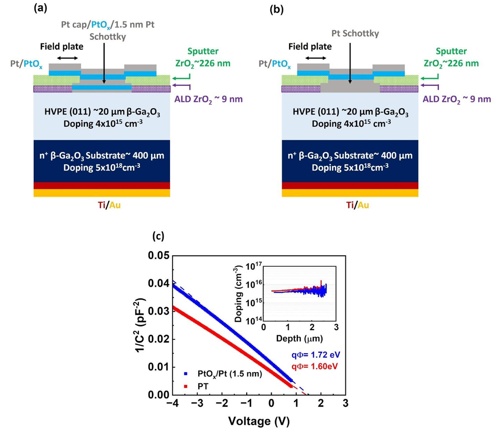
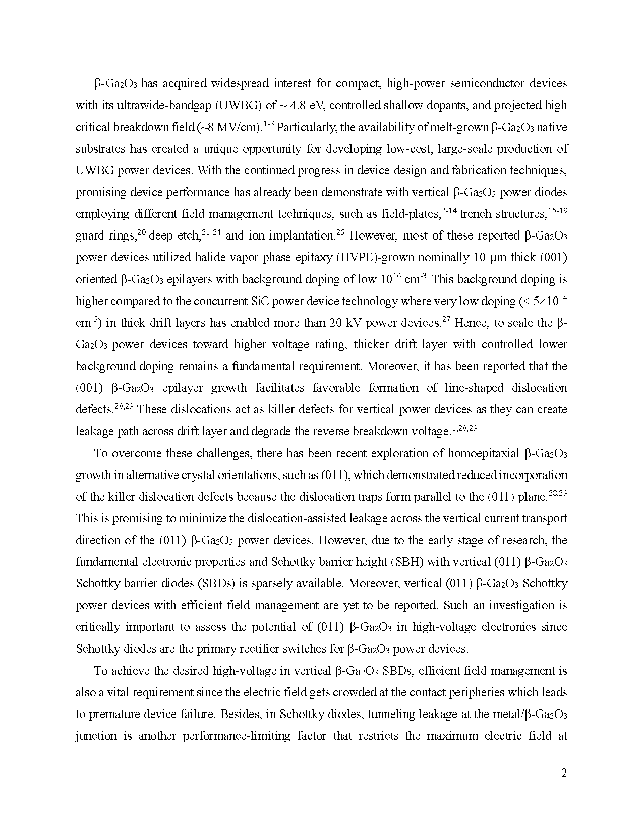
Fig. 1. Schematic of the field-plate vertical (011) β-Ga2O3 Schottky diode of 100 μm diameter and a high-κ ZrO2 field plate with (a) composite Pt cap/PtOx/Pt (1.5 nm) Schottky contact and (b) Pt Schottky contact. (c) The extracted SBH from 1/C2-V analysis for both SBDs, with the inset depicting the extracted doping concentration.
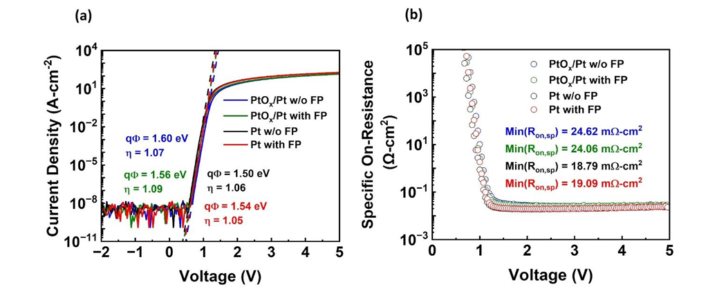
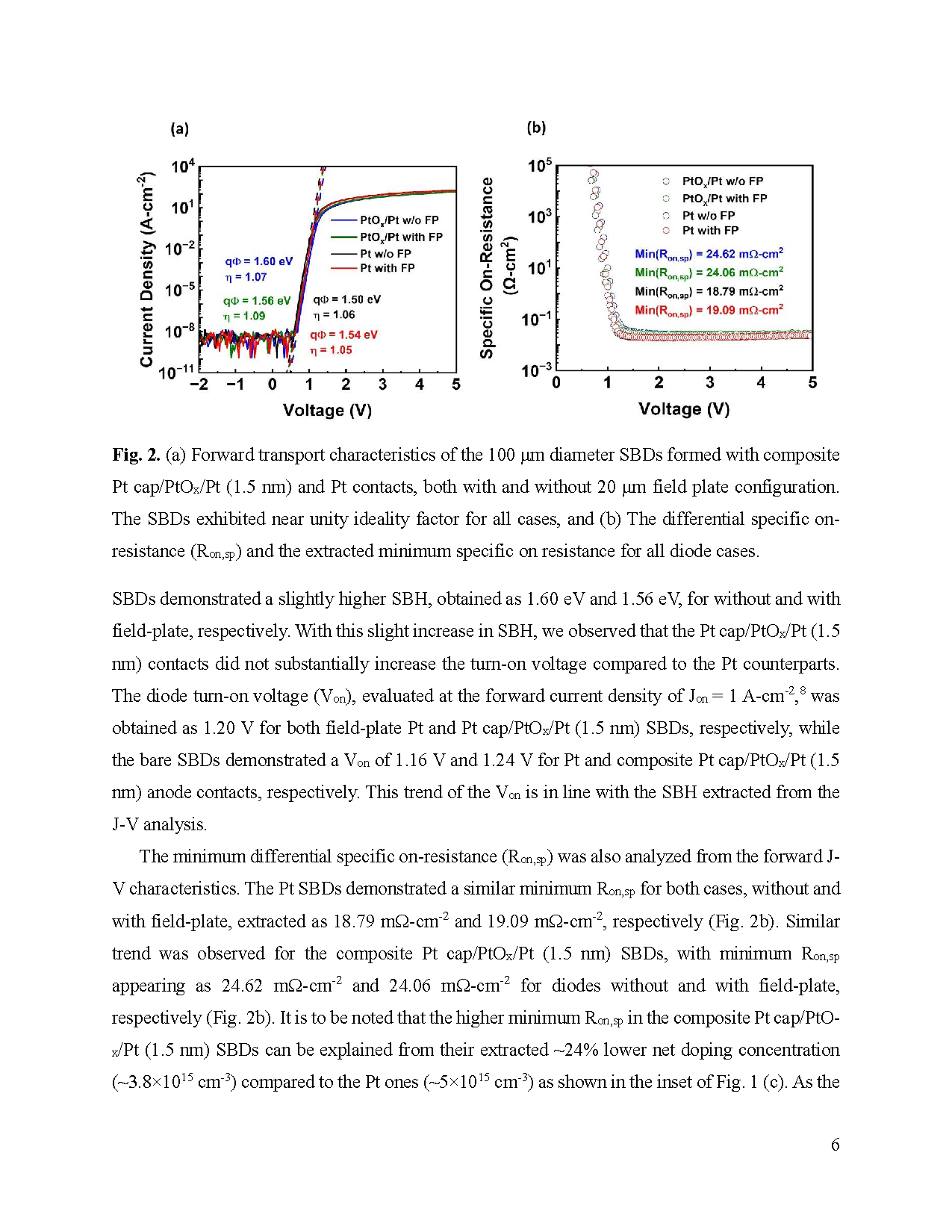
Fig. 2. (a) Forward transport characteristics of the 100 μm diameter SBDs formed with composite Pt cap/PtOx/Pt (1.5 nm) and Pt contacts, both with and without 20 μm field plate configuration. The SBDs exhibited near unity ideality factor for all cases, and (b) The differential specific on resistance (Ron,sp) and the extracted minimum specific on resistance for all diode cases.
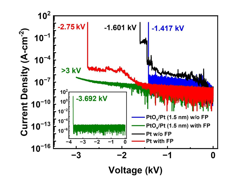
Fig. 3. Reverse J-V characteristics of 100 μm diameter composite Pt cap/PtOx/Pt (1.5 nm) and Pt SBD both with and without 20 μm field plate. Without field-plate, both composite Pt cap/PtOx/Pt (1.5 nm) and Pt SBD show similar breakdown voltages in the range of 1.4-1.6 kV. With field plate, the composite Pt cap/PtOx/Pt (1.5 nm) device shows consistently reduced reverse leakage current and higher breakdown voltage beyond 3 kV. The inset shows the breakdown of the composite Pt cap/PtOx/Pt (1.5 nm) with FP device, which was characterized using a separate parametric analyzer at UCSB capable of measuring beyond 3 kV but had a higher noise floor.
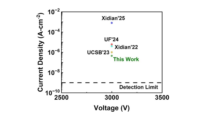
Fig. 4. Benchmark plot of reverse leakage current density at 3 kV, comparing our work on vertical (011) β-Ga2O3 SBDs and the reported vertical β-Ga2O3 SBDs on (001) epiwafers.
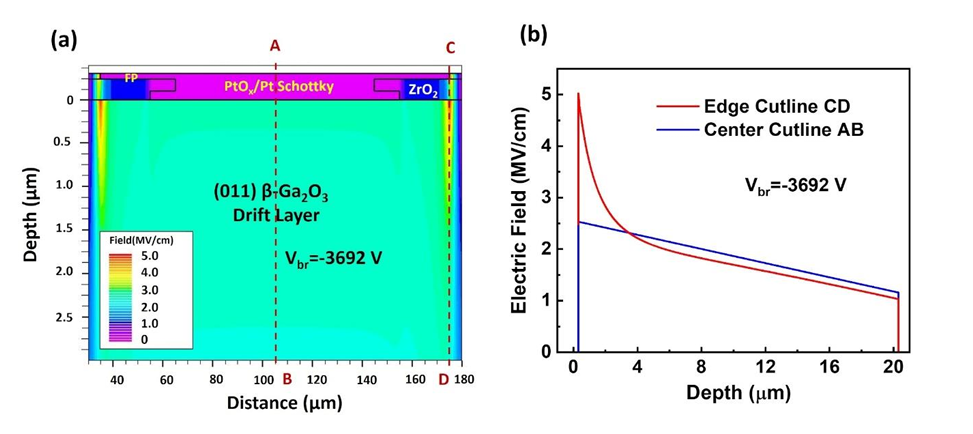
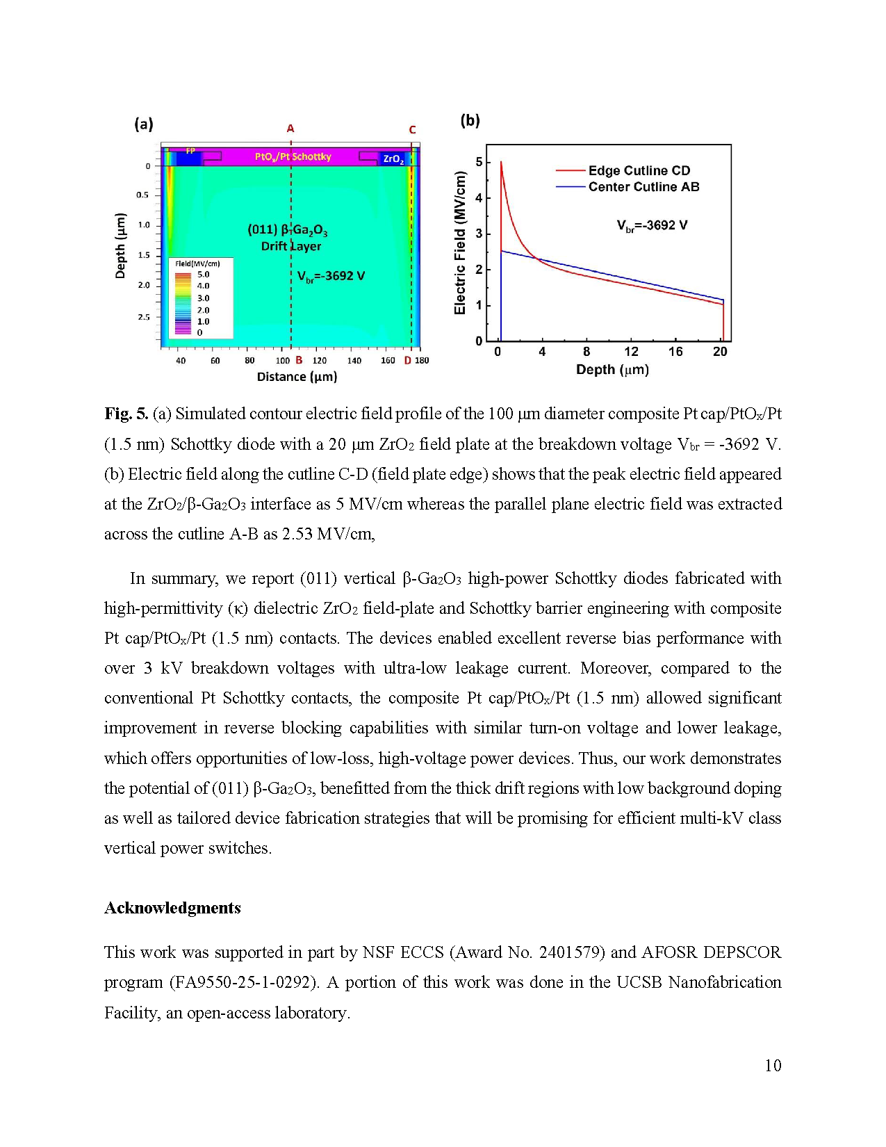
Fig. 5. (a) Simulated contour electric field profile of the 100 μm diameter composite Pt cap/PtOx/Pt (1.5 nm) Schottky diode with a 20 μm ZrO2 field plate at the breakdown voltage Vbr = -3692 V. (b) Electric field along the cutline C-D (field plate edge) shows that the peak electric field appeared at the ZrO2/β-Ga2O3 interface as 5 MV/cm whereas the parallel plane electric field was extracted across the cutline A-B as 2.53 MV/cm.
DOI:
doi.org/10.48550/arXiv.2510.25695